|
công cụ tìm kiếm bảng dữ liệu linh kiện điện tử |
|
|
công cụ tìm kiếm bảng dữ liệu linh kiện điện tử |
|
PIC18F2680ISPSQTP bảng dữ liệu(PDF) 30 Page - Microchip Technology |
|
|
|||||||||||||||||||||||||||||
PIC18F2680ISPSQTP bảng dữ liệu(HTML) 30 Page - Microchip Technology |
|
|
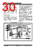
30 / 482 page  PIC18F2585/2680/4585/4680 DS39625C-page 28 Preliminary © 2007 Microchip Technology Inc. 2.7 Clock Sources and Oscillator Switching Like previous PIC18 devices, the PIC2585/2680/ 4585/4680 family includes a feature that allows the device clock source to be switched from the main oscillator to an alternate low-frequency clock source. PIC18F2585/2680/4585/4680 devices offer two alter- nate clock sources. When an alternate clock source is enabled, the various power managed operating modes are available. Essentially, there are three clock sources for these devices: • Primary oscillators • Secondary oscillators • Internal oscillator block The primary oscillators include the External Crystal and Resonator modes, the External RC modes, the External Clock modes and the internal oscillator block. The particular mode is defined by the FOSC3:FOSC0 Configuration bits. The details of these modes are covered earlier in this chapter. The secondary oscillators are those external sources not connected to the OSC1 or OSC2 pins. These sources may continue to operate even after the controller is placed in a power managed mode. PIC18F2585/2680/4585/4680 devices offer the Timer1 oscillator as a secondary oscillator. This oscillator, in all power managed modes, is often the time base for functions such as a real-time clock. Most often, a 32.768 kHz watch crystal is connected between the RC0/T1OSO/T13CKI and RC1/T1OSI pins. Like the LP mode oscillator circuit, loading capacitors are also connected from each pin to ground. The Timer1 oscillator is discussed in greater detail in Section 12.3 “Timer1 Oscillator”. In addition to being a primary clock source, the internal oscillator block is available as a power managed mode clock source. The INTRC source is also used as the clock source for several special features, such as the WDT and Fail-Safe Clock Monitor. The clock sources for the PIC18F2585/2680/4585/4680 devices are shown in Figure 2-8. See Section 24.0 “Special Features of the CPU” for Configuration register details. FIGURE 2-8: PIC18F2585/2680/4585/4680 CLOCK DIAGRAM PIC18FX585/X680 4 x PLL FOSC3:FOSC0 Secondary Oscillator T1OSCEN Enable Oscillator T1OSO T1OSI Clock Source Option for other Modules OSC1 OSC2 Sleep Primary Oscillator HSPLL, INTOSC/PLL LP, XT, HS, RC, EC T1OSC CPU Peripherals IDLEN 8 MHz 4 MHz 2 MHz 1 MHz 500 kHz 125 kHz 250 kHz OSCCON<6:4> 111 110 101 100 011 010 001 000 31 kHz INTRC Source Internal Oscillator Block WDT, PWRT, FSCM 8 MHz Internal Oscillator (INTOSC) OSCCON<6:4> Clock Control OSCCON<1:0> Source 8 MHz 31 kHz (INTRC) OSCTUNE<6> 0 1 OSCTUNE<7> and Two-Speed Startup |
|
Link URL |
| Cho đến nay ALLDATASHEET có giúp ích cho doanh nghiệp của bạn hay không? [ DONATE ] |
Alldatasheet là | Quảng cáo | Liên lạc với chúng tôi | Chính sách bảo mật | Liên kết đến bảng dữ liệu | Trao đổi link | Tìm kiếm theo nhà sản xuất All Rights Reserved©Alldatasheet.com |
| Russian : Alldatasheetru.com | Korean : Alldatasheet.co.kr | Spanish : Alldatasheet.es | French : Alldatasheet.fr | Italian : Alldatasheetit.com Portuguese : Alldatasheetpt.com | Polish : Alldatasheet.pl | Vietnamese : Alldatasheet.vn Indian : Alldatasheet.in | Mexican : Alldatasheet.com.mx | British : Alldatasheet.co.uk | New Zealand : Alldatasheet.co.nz |
|
Family Site : ic2ic.com |
icmetro.com |
 Vietnamese ▼
 English
 Chinese
 German
 Japanese
 Russian
 Korean
 Spanish
 French
 Italian
 Portuguese
 Polish
 Vietnamese
 Indian
 Mexican
 British
 New Zealand