|
công cụ tìm kiếm bảng dữ liệu linh kiện điện tử |
|
|
công cụ tìm kiếm bảng dữ liệu linh kiện điện tử |
|
PIC16F1516 bảng dữ liệu(PDF) 192 Page - Microchip Technology |
|
|
|||||||||||||||||||||||||||||
PIC16F1516 bảng dữ liệu(HTML) 192 Page - Microchip Technology |
|
|
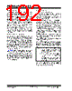
192 / 344 page  PIC16(L)F1516/7/8/9 DS41452B-page 192 Preliminary 2011 Microchip Technology Inc. 21.2.4 SPI SLAVE MODE In Slave mode, the data is transmitted and received as external clock pulses appear on SCK. When the last bit is latched, the SSPIF interrupt flag bit is set. Before enabling the module in SPI Slave mode, the clock line must match the proper Idle state. The clock line can be observed by reading the SCK pin. The Idle state is determined by the CKP bit of the SSPCON1 register. While in Slave mode, the external clock is supplied by the external clock source on the SCK pin. This external clock must meet the minimum high and low times as specified in the electrical specifications. While in Sleep mode, the slave can transmit/receive data. The shift register is clocked from the SCK pin input and when a byte is received, the device will gen- erate an interrupt. If enabled, the device will wake-up from Sleep. 21.2.4.1 Daisy-Chain Configuration The SPI bus can sometimes be connected in a daisy-chain configuration. The first slave output is con- nected to the second slave input, the second slave output is connected to the third slave input, and so on. The final slave output is connected to the master input. Each slave sends out, during a second group of clock pulses, an exact copy of what was received during the first group of clock pulses. The whole chain acts as one large communication shift register. The daisy-chain feature only requires a single Slave Select line from the master device. Figure 21-7 shows the block diagram of a typical daisy-chain connection when operating in SPI Mode. In a daisy-chain configuration, only the most recent byte on the bus is required by the slave. Setting the BOEN bit of the SSPCON3 register will enable writes to the SSPBUF register, even if the previous byte has not been read. This allows the software to ignore data that may not apply to it. 21.2.5 SLAVE SELECT SYNCHRONIZATION The Slave Select can also be used to synchronize com- munication. The Slave Select line is held high until the master device is ready to communicate. When the Slave Select line is pulled low, the slave knows that a new transmission is starting. If the slave fails to receive the communication properly, it will be reset at the end of the transmission, when the Slave Select line returns to a high state. The slave is then ready to receive a new transmission when the Slave Select line is pulled low again. If the Slave Select line is not used, there is a risk that the slave will even- tually become out of sync with the master. If the slave misses a bit, it will always be one bit off in future trans- missions. Use of the Slave Select line allows the slave and master to align themselves at the beginning of each transmission. The SS pin allows a Synchronous Slave mode. The SPI must be in Slave mode with SS pin control enabled (SSPCON1<3:0> = 0100). When the SS pin is low, transmission and reception are enabled and the SDO pin is driven. When the SS pin goes high, the SDO pin is no longer driven, even if in the middle of a transmitted byte and becomes a floating output. External pull-up/pull-down resistors may be desirable depending on the applica- tion. When the SPI module resets, the bit counter is forced to ‘0’. This can be done by either forcing the SS pin to a high level or clearing the SSPEN bit. Note 1: When the SPI is in Slave mode with SS pin control enabled (SSPCON1<3:0> = 0100 ), the SPI module will reset if the SS pin is set to VDD. 2: When the SPI is used in Slave mode with CKE set; the user must enable SS pin control. 3: While operated in SPI Slave mode the SMP bit of the SSPSTAT register must remain clear. |
|
Link URL |
| Cho đến nay ALLDATASHEET có giúp ích cho doanh nghiệp của bạn hay không? [ DONATE ] |
Alldatasheet là | Quảng cáo | Liên lạc với chúng tôi | Chính sách bảo mật | Liên kết đến bảng dữ liệu | Trao đổi link | Tìm kiếm theo nhà sản xuất All Rights Reserved©Alldatasheet.com |
| Russian : Alldatasheetru.com | Korean : Alldatasheet.co.kr | Spanish : Alldatasheet.es | French : Alldatasheet.fr | Italian : Alldatasheetit.com Portuguese : Alldatasheetpt.com | Polish : Alldatasheet.pl | Vietnamese : Alldatasheet.vn Indian : Alldatasheet.in | Mexican : Alldatasheet.com.mx | British : Alldatasheet.co.uk | New Zealand : Alldatasheet.co.nz |
|
Family Site : ic2ic.com |
icmetro.com |
 Vietnamese ▼
 English
 Chinese
 German
 Japanese
 Russian
 Korean
 Spanish
 French
 Italian
 Portuguese
 Polish
 Vietnamese
 Indian
 Mexican
 British
 New Zealand