|
công cụ tìm kiếm bảng dữ liệu linh kiện điện tử |
|
|
công cụ tìm kiếm bảng dữ liệu linh kiện điện tử |
|
PIC16F1516 bảng dữ liệu(PDF) 97 Page - Microchip Technology |
|
|
|||||||||||||||||||||||||||||
PIC16F1516 bảng dữ liệu(HTML) 97 Page - Microchip Technology |
|
|
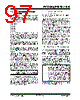
97 / 344 page  2011 Microchip Technology Inc. Preliminary DS41452B-page 97 PIC16(L)F1516/7/8/9 11.0 FLASH PROGRAM MEMORY CONTROL The Flash program memory is readable and writable during normal operation over the full VDD range. Program memory is indirectly addressed using Special Function Registers (SFRs). The SFRs used to access program memory are: •PMCON1 •PMCON2 •PMDATL •PMDATH • PMADRL •PMADRH When accessing the program memory, the PMDATH:PMDATL register pair forms a 2-byte word that holds the 14-bit data for read/write, and the PMDATH:PMDATL register pair forms a 2-byte word that holds the 15-bit address of the program memory location being read. The write time is controlled by an on-chip timer. The write/ erase voltages are generated by an on-chip charge pump rated to operate over the operating voltage range of the device. The Flash program memory can be protected in two ways; by code protection (CP bit in Configuration Word 1) and write protection (WRT<1:0> bits in Configuration Word 2). Code protection (CP = 0)(1), disables access, reading and writing, to the Flash program memory via external device programmers. Code protection does not affect the self-write and erase functionality. Code protection can only be reset by a device programmer performing a Bulk Erase to the device, clearing all Flash program memory, Configuration bits and User IDs. Write protection prohibits self-write and erase to a portion or all of the Flash program memory as defined by the bits WRT<1:0>. Write protection does not affect a device programmers ability to read, write or erase the device. 11.1 PMADRL and PMADRH Registers The PMADRH:PMADRL register pair can address up to a maximum of 32K words of program memory. When selecting a program address value, the MSB of the address is written to the PMADRH register and the LSB is written to the PMADRL register. 11.1.1 PMCON1 AND PMCON2 REGISTERS PMCON1 is the control register for Flash program memory accesses. Control bits RD and WR initiate read and write, respectively. These bits cannot be cleared, only set, in software. They are cleared by hardware at completion of the read or write operation. The inability to clear the WR bit in software prevents the accidental, premature termination of a write operation. The WREN bit, when set, will allow a write operation to occur. On power-up, the WREN bit is clear. The WRERR bit is set when a write operation is interrupted by a Reset during normal operation. In these situations, following Reset, the user can check the WRERR bit and execute the appropriate error handling routine. The PMCON2 register is a write-only register. Attempting to read the PMCON2 register will return all ‘0’s. To enable writes to the program memory, a specific pattern (the unlock sequence), must be written to the PMCON2 register. The required unlock sequence prevents inadvertent writes to the program memory write latches and Flash program memory. 11.2 Flash Program Memory Overview It is important to understand the Flash program memory structure for erase and programming operations. Flash program memory is arranged in rows. A row consists of a fixed number of 14-bit program memory words. A row is the minimum size that can be erased by user software. After a row has been erased, the user can reprogram all or a portion of this row. Data to be written into the program memory row is written to 14-bit wide data write latches. These write latches are not directly accessible to the user, but may be loaded via sequential writes to the PMDATH:PMDATL register pair. See Table 11-1 for Erase Row size and the number of write latches for Flash program memory. Note 1: Code protection of the entire Flash program memory array is enabled by clearing the CP bit of Configuration Word 1. Note: If the user wants to modify only a portion of a previously programmed row, then the contents of the entire row must be read and saved in RAM prior to the erase. Then, new data and retained data can be written into the write latches to reprogram the row of Flash program memory. How- ever, any unprogrammed locations can be written without first erasing the row. In this case, it is not necessary to save and rewrite the other previously programmed locations. |
|
Link URL |
| Cho đến nay ALLDATASHEET có giúp ích cho doanh nghiệp của bạn hay không? [ DONATE ] |
Alldatasheet là | Quảng cáo | Liên lạc với chúng tôi | Chính sách bảo mật | Liên kết đến bảng dữ liệu | Trao đổi link | Tìm kiếm theo nhà sản xuất All Rights Reserved©Alldatasheet.com |
| Russian : Alldatasheetru.com | Korean : Alldatasheet.co.kr | Spanish : Alldatasheet.es | French : Alldatasheet.fr | Italian : Alldatasheetit.com Portuguese : Alldatasheetpt.com | Polish : Alldatasheet.pl | Vietnamese : Alldatasheet.vn Indian : Alldatasheet.in | Mexican : Alldatasheet.com.mx | British : Alldatasheet.co.uk | New Zealand : Alldatasheet.co.nz |
|
Family Site : ic2ic.com |
icmetro.com |
 Vietnamese ▼
 English
 Chinese
 German
 Japanese
 Russian
 Korean
 Spanish
 French
 Italian
 Portuguese
 Polish
 Vietnamese
 Indian
 Mexican
 British
 New Zealand