|
công cụ tìm kiếm bảng dữ liệu linh kiện điện tử |
|
|
công cụ tìm kiếm bảng dữ liệu linh kiện điện tử |
|
PIC16F1516 bảng dữ liệu(PDF) 101 Page - Microchip Technology |
|
|
|||||||||||||||||||||||||||||
PIC16F1516 bảng dữ liệu(HTML) 101 Page - Microchip Technology |
|
|
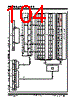
101 / 344 page  2011 Microchip Technology Inc. Preliminary DS41452B-page 101 PIC16(L)F1516/7/8/9 11.2.3 ERASING FLASH PROGRAM MEMORY While executing code, program memory can only be erased by rows. To erase a row: 1. Load the PMADRH:PMADRL register pair with any address within the row to be erased. 2. Clear the CFGS bit of the PMCON1 register. 3. Set the FREE and WREN bits of the PMCON1 register. 4. Write 55h, then AAh, to PMCON2 (Flash programming unlock sequence). 5. Set control bit WR of the PMCON1 register to begin the erase operation. See Example 11-2. After the “BSF PMCON1,WR” instruction, the processor requires two cycles to set up the erase operation. The user must place two NOP instructions after the WR bit is set. The processor will halt internal operations for the typical 2 ms erase time. This is not Sleep mode as the clocks and peripherals will continue to run. After the erase cycle, the processor will resume operation with the third instruction after the PMCON1 write instruction. FIGURE 11-4: FLASH PROGRAM MEMORY ERASE FLOWCHART Disable Interrupts (GIE = 0) Start ERASE Operation Select Program or Configuration Memory (CFGS) Select Row Address (PMADRH:PMADRL) Select ERASE Operation (FREE = 1) Enable Write/Erase Operation (WREN = 1) Unlock Sequence (FIGURE x-x) Disable Write/Erase Operation (WREN = 0) Re-enable Interrupts (GIE = 1) End ERASE Operation CPU stalls while ERASE operation completes (2ms typical) Figure 11-3 |
|
Link URL |
| Cho đến nay ALLDATASHEET có giúp ích cho doanh nghiệp của bạn hay không? [ DONATE ] |
Alldatasheet là | Quảng cáo | Liên lạc với chúng tôi | Chính sách bảo mật | Liên kết đến bảng dữ liệu | Trao đổi link | Tìm kiếm theo nhà sản xuất All Rights Reserved©Alldatasheet.com |
| Russian : Alldatasheetru.com | Korean : Alldatasheet.co.kr | Spanish : Alldatasheet.es | French : Alldatasheet.fr | Italian : Alldatasheetit.com Portuguese : Alldatasheetpt.com | Polish : Alldatasheet.pl | Vietnamese : Alldatasheet.vn Indian : Alldatasheet.in | Mexican : Alldatasheet.com.mx | British : Alldatasheet.co.uk | New Zealand : Alldatasheet.co.nz |
|
Family Site : ic2ic.com |
icmetro.com |
 Vietnamese ▼
 English
 Chinese
 German
 Japanese
 Russian
 Korean
 Spanish
 French
 Italian
 Portuguese
 Polish
 Vietnamese
 Indian
 Mexican
 British
 New Zealand