|
công cụ tìm kiếm bảng dữ liệu linh kiện điện tử |
|
|
công cụ tìm kiếm bảng dữ liệu linh kiện điện tử |
|
PIC16F1516 bảng dữ liệu(PDF) 172 Page - Microchip Technology |
|
|
|||||||||||||||||||||||||||||
PIC16F1516 bảng dữ liệu(HTML) 172 Page - Microchip Technology |
|
|
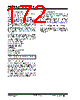
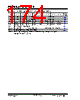
172 / 344 page  PIC16(L)F1516/7/8/9 DS41452B-page 172 Preliminary 2011 Microchip Technology Inc. 19.1 Timer2 Operation The clock input to the Timer2 modules is the system instruction clock (FOSC/4). TMR2 increments from 00h on each clock edge. A 4-bit counter/prescaler on the clock input allows direct input, divide-by-4 and divide-by-16 prescale options. These options are selected by the prescaler control bits, T2CKPS<1:0> of the T2CON register. The value of TMR2 is compared to that of the Period register, PR2, on each clock cycle. When the two values match, the comparator generates a match signal as the timer output. This signal also resets the value of TMR2 to 00h on the next cycle and drives the output counter/postscaler (see Section 19.2 “Timer2 Interrupt” ). The TMR2 and PR2 registers are both directly readable and writable. The TMR2 register is cleared on any device Reset, whereas the PR2 register initializes to FFh. Both the prescaler and postscaler counters are cleared on the following events: • a write to the TMR2 register • a write to the T2CON register • Power-on Reset (POR) • Brown-out Reset (BOR) •MCLR Reset • Watchdog Timer (WDT) Reset • Stack Overflow Reset • Stack Underflow Reset • RESET Instruction 19.2 Timer2 Interrupt Timer2 can also generate an optional device interrupt. The Timer2 output signal (TMR2-to-PR2 match) provides the input for the 4-bit counter/postscaler. This counter generates the TMR2 match interrupt flag which is latched in TMR2IF of the PIR1 register. The interrupt is enabled by setting the TMR2 Match Interrupt Enable bit, TMR2IE of the PIE1 register. A range of 16 postscale options (from 1:1 through 1:16 inclusive) can be selected with the postscaler control bits, T2OUTPS<3:0>, of the T2CON register. 19.3 Timer2 Output The unscaled output of TMR2 is available primarily to the CCP1 module, where it is used as a time base for operations in PWM mode. Timer2 can be optionally used as the shift clock source for the MSSP module operating in SPI mode. Additional information is provided in Section 21.0 “Master Synchronous Serial Port (MSSP) Module” 19.4 Timer2 Operation During Sleep Timer2 cannot be operated while the processor is in Sleep mode. The contents of the TMR2 and PR2 registers will remain unchanged while the processor is in Sleep mode. Note: TMR2 is not cleared when T2CON is written. |
|
Link URL |
| Cho đến nay ALLDATASHEET có giúp ích cho doanh nghiệp của bạn hay không? [ DONATE ] |
Alldatasheet là | Quảng cáo | Liên lạc với chúng tôi | Chính sách bảo mật | Liên kết đến bảng dữ liệu | Trao đổi link | Tìm kiếm theo nhà sản xuất All Rights Reserved©Alldatasheet.com |
| Russian : Alldatasheetru.com | Korean : Alldatasheet.co.kr | Spanish : Alldatasheet.es | French : Alldatasheet.fr | Italian : Alldatasheetit.com Portuguese : Alldatasheetpt.com | Polish : Alldatasheet.pl | Vietnamese : Alldatasheet.vn Indian : Alldatasheet.in | Mexican : Alldatasheet.com.mx | British : Alldatasheet.co.uk | New Zealand : Alldatasheet.co.nz |
|
Family Site : ic2ic.com |
icmetro.com |
 Vietnamese ▼
 English
 Chinese
 German
 Japanese
 Russian
 Korean
 Spanish
 French
 Italian
 Portuguese
 Polish
 Vietnamese
 Indian
 Mexican
 British
 New Zealand