|
công cụ tìm kiếm bảng dữ liệu linh kiện điện tử |
|
|
công cụ tìm kiếm bảng dữ liệu linh kiện điện tử |
|
PIC16F1516 bảng dữ liệu(PDF) 115 Page - Microchip Technology |
|
|
|||||||||||||||||||||||||||||
PIC16F1516 bảng dữ liệu(HTML) 115 Page - Microchip Technology |
|
|
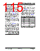
115 / 344 page  2010 Microchip Technology Inc. Preliminary DS41452B-page 115 PIC16(L)F1516/7/8/9 12.2 PORTA Registers PORTA is a 8-bit wide, bidirectional port. The corresponding data direction register is TRISA (Register 12-3). Setting a TRISA bit (= 1) will make the corresponding PORTA pin an input (i.e., disable the output driver). Clearing a TRISA bit (= 0) will make the corresponding PORTA pin an output (i.e., enables output driver and puts the contents of the output latch on the selected pin). Example 12-1 shows how to initialize an I/O port. Reading the PORTA register (Register 12-2) reads the status of the pins, whereas writing to it will write to the PORT latch. All write operations are read-modify-write operations. Therefore, a write to a port implies that the port pins are read, this value is modified and then written to the PORT data latch (LATA). The TRISA register (Register 12-3) controls the PORTA pin output drivers, even when they are being used as analog inputs. The user should ensure the bits in the TRISA register are maintained set when using them as analog inputs. I/O pins configured as analog input always read ‘0’. 12.2.1 ANSELA REGISTER The ANSELA register (Register 12-5) is used to configure the Input mode of an I/O pin to analog. Setting the appropriate ANSELA bit high will cause all digital reads on the pin to be read as ‘0’ and allow analog functions on the pin to operate correctly. The state of the ANSELA bits has no affect on digital output functions. A pin with TRIS clear and ANSEL set will still operate as a digital output, but the Input mode will be analog. This can cause unexpected behavior when executing read-modify-write instructions on the affected port. 12.2.2 PORTA FUNCTIONS AND OUTPUT PRIORITIES Each PORTA pin is multiplexed with other functions. The pins, their combined functions and their output priorities are shown in Table 12-2. When multiple outputs are enabled, the actual pin control goes to the peripheral with the highest priority. Analog input functions, such as ADC, are not shown in the priority lists. These inputs are active when the I/O pin is set for Analog mode using the ANSELx registers. Digital output functions may control the pin when it is in Analog mode with the priority shown in Table 12-2. Note: The ANSELA register must be initialized to configure an analog channel as a digital input. Pins configured as analog inputs will read ‘0’. TABLE 12-2: PORTA OUTPUT PRIORITY Pin Name Function Priority(1) RA0 RA0 RA1 RA1 RA2 RA2 RA3 RA3 RA4 RA4 RA5 VCAP (PIC16F151X only) RA5 RA6 CLKOUT OSC2 RA6 RA7 RA7 Note 1: Priority listed from highest to lowest. |
|
Link URL |
| Cho đến nay ALLDATASHEET có giúp ích cho doanh nghiệp của bạn hay không? [ DONATE ] |
Alldatasheet là | Quảng cáo | Liên lạc với chúng tôi | Chính sách bảo mật | Liên kết đến bảng dữ liệu | Trao đổi link | Tìm kiếm theo nhà sản xuất All Rights Reserved©Alldatasheet.com |
| Russian : Alldatasheetru.com | Korean : Alldatasheet.co.kr | Spanish : Alldatasheet.es | French : Alldatasheet.fr | Italian : Alldatasheetit.com Portuguese : Alldatasheetpt.com | Polish : Alldatasheet.pl | Vietnamese : Alldatasheet.vn Indian : Alldatasheet.in | Mexican : Alldatasheet.com.mx | British : Alldatasheet.co.uk | New Zealand : Alldatasheet.co.nz |
|
Family Site : ic2ic.com |
icmetro.com |
 Vietnamese ▼
 English
 Chinese
 German
 Japanese
 Russian
 Korean
 Spanish
 French
 Italian
 Portuguese
 Polish
 Vietnamese
 Indian
 Mexican
 British
 New Zealand