|
công cụ tìm kiếm bảng dữ liệu linh kiện điện tử |
|
|
công cụ tìm kiếm bảng dữ liệu linh kiện điện tử |
|
PIC16F1516 bảng dữ liệu(PDF) 139 Page - Microchip Technology |
|
|
|||||||||||||||||||||||||||||
PIC16F1516 bảng dữ liệu(HTML) 139 Page - Microchip Technology |
|
|
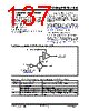
139 / 344 page  2011 Microchip Technology Inc. Preliminary DS41452B-page 139 PIC16(L)F1516/7/8/9 15.0 TEMPERATURE INDICATOR MODULE This family of devices is equipped with a temperature circuit designed to measure the operating temperature of the silicon die. The circuit’s range of operating temperature falls between of -40°C and +85°C. The output is a voltage that is proportional to the device temperature. The output of the temperature indicator is internally connected to the device ADC. The circuit may be used as a temperature threshold detector or a more accurate temperature indicator, depending on the level of calibration performed. A one- point calibration allows the circuit to indicate a temperature closely surrounding that point. A two-point calibration allows the circuit to sense the entire range of temperature more accurately. Reference Application Note AN1333, “Use and Calibration of the Internal Temperature Indicator ” (DS01333) for more details regarding the calibration process. 15.1 Circuit Operation Figure 15-1 shows a simplified block diagram of the temperature circuit. The proportional voltage output is achieved by measuring the forward voltage drop across multiple silicon junctions. Equation 15-1 describes the output characteristics of the temperature indicator. EQUATION 15-1: VOUT RANGES The temperature sense circuit is integrated with the Fixed Voltage Reference (FVR) module. See Section 14.0 “Fixed Voltage Reference (FVR)” for more information. The circuit is enabled by setting the TSEN bit of the FVRCON register. When disabled, the circuit draws no current. The circuit operates in either high or low range. The high range, selected by setting the TSRNG bit of the FVRCON register, provides a wider output voltage. This provides more resolution over the temperature range, but may be less consistent from part to part. This range requires a higher bias voltage to operate and thus, a higher VDD is needed. The low range is selected by clearing the TSRNG bit of the FVRCON register. The low range generates a lower voltage drop and thus, a lower bias voltage is needed to operate the circuit. The low range is provided for low voltage operation. FIGURE 15-1: TEMPERATURE CIRCUIT DIAGRAM 15.2 Minimum Operating VDD vs. Minimum Sensing Temperature When the temperature circuit is operated in low range, the device may be operated at any operating voltage that is within specifications. When the temperature circuit is operated in high range, the device operating voltage, VDD, must be high enough to ensure that the temperature circuit is correctly biased. Table 15-1 shows the recommended minimum VDD vs. range setting. TABLE 15-1: RECOMMENDED VDD VS. RANGE 15.3 Temperature Output The output of the circuit is measured using the internal analog to digital converter. A channel is reserved for the temperature circuit output. Refer to Section 16.0 “Analog-to-Digital Converter (ADC) Module” for detailed information. 15.4 ADC Aquisition Time To ensure accurate temperature measurements, the user must wait at least 200 s after the ADC input multiplexer is connected to the temperature indicator output before the conversion is performed. In addition, the user must wait 200 s between sequential conversions of the temperature indicator output. High Range: VOUT = VDD - 4VT Low Range: VOUT = VDD - 2VT Min. VDD, TSRNG = 1 Min. VDD, TSRNG = 0 3.6V 1.8V TSEN ADC MUX TSRNG VDD ADC CHS bits (ADCON0 register) n VOUT |
|
Link URL |
| Cho đến nay ALLDATASHEET có giúp ích cho doanh nghiệp của bạn hay không? [ DONATE ] |
Alldatasheet là | Quảng cáo | Liên lạc với chúng tôi | Chính sách bảo mật | Liên kết đến bảng dữ liệu | Trao đổi link | Tìm kiếm theo nhà sản xuất All Rights Reserved©Alldatasheet.com |
| Russian : Alldatasheetru.com | Korean : Alldatasheet.co.kr | Spanish : Alldatasheet.es | French : Alldatasheet.fr | Italian : Alldatasheetit.com Portuguese : Alldatasheetpt.com | Polish : Alldatasheet.pl | Vietnamese : Alldatasheet.vn Indian : Alldatasheet.in | Mexican : Alldatasheet.com.mx | British : Alldatasheet.co.uk | New Zealand : Alldatasheet.co.nz |
|
Family Site : ic2ic.com |
icmetro.com |
 Vietnamese ▼
 English
 Chinese
 German
 Japanese
 Russian
 Korean
 Spanish
 French
 Italian
 Portuguese
 Polish
 Vietnamese
 Indian
 Mexican
 British
 New Zealand