|
công cụ tìm kiếm bảng dữ liệu linh kiện điện tử |
|
|
công cụ tìm kiếm bảng dữ liệu linh kiện điện tử |
|
PIC16F1516 bảng dữ liệu(PDF) 220 Page - Microchip Technology |
|
|
|||||||||||||||||||||||||||||
PIC16F1516 bảng dữ liệu(HTML) 220 Page - Microchip Technology |
|
|
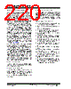
220 / 344 page  PIC16(L)F1516/7/8/9 DS41452B-page 220 Preliminary 2011 Microchip Technology Inc. 21.6.6 I2C MASTER MODE TRANSMISSION Transmission of a data byte, a 7-bit address or the other half of a 10-bit address is accomplished by simply writing a value to the SSPBUF register. This action will set the Buffer Full flag bit, BF and allow the Baud Rate Generator to begin counting and start the next trans- mission. Each bit of address/data will be shifted out onto the SDA pin after the falling edge of SCL is asserted. SCL is held low for one Baud Rate Generator rollover count (TBRG). Data should be valid before SCL is released high. When the SCL pin is released high, it is held that way for TBRG. The data on the SDA pin must remain stable for that duration and some hold time after the next falling edge of SCL. After the eighth bit is shifted out (the falling edge of the eighth clock), the BF flag is cleared and the master releases SDA. This allows the slave device being addressed to respond with an ACK bit during the ninth bit time if an address match occurred, or if data was received prop- erly. The status of ACK is written into the ACKSTAT bit on the rising edge of the ninth clock. If the master receives an Acknowledge, the Acknowledge Status bit, ACKSTAT, is cleared. If not, the bit is set. After the ninth clock, the SSPIF bit is set and the master clock (Baud Rate Generator) is suspended until the next data byte is loaded into the SSPBUF, leaving SCL low and SDA unchanged (Figure 21-27). After the write to the SSPBUF, each bit of the address will be shifted out on the falling edge of SCL until all seven address bits and the R/W bit are completed. On the falling edge of the eighth clock, the master will release the SDA pin, allowing the slave to respond with an Acknowledge. On the falling edge of the ninth clock, the master will sample the SDA pin to see if the address was recognized by a slave. The status of the ACK bit is loaded into the ACKSTAT Status bit of the SSPCON2 register. Following the falling edge of the ninth clock transmission of the address, the SSPIF is set, the BF flag is cleared and the Baud Rate Generator is turned off until another write to the SSPBUF takes place, hold- ing SCL low and allowing SDA to float. 21.6.6.1 BF Status Flag In Transmit mode, the BF bit of the SSPSTAT register is set when the CPU writes to SSPBUF and is cleared when all 8 bits are shifted out. 21.6.6.2 WCOL Status Flag If the user writes the SSPBUF when a transmit is already in progress (i.e., SSPSR is still shifting out a data byte), the WCOL is set and the contents of the buf- fer are unchanged (the write does not occur). WCOL must be cleared by software before the next transmission. 21.6.6.3 ACKSTAT Status Flag In Transmit mode, the ACKSTAT bit of the SSPCON2 register is cleared when the slave has sent an Acknowl- edge (ACK = 0) and is set when the slave does not Acknowledge (ACK = 1). A slave sends an Acknowl- edge when it has recognized its address (including a general call), or when the slave has properly received its data. 21.6.6.4 Typical transmit sequence: 1. The user generates a Start condition by setting the SEN bit of the SSPCON2 register. 2. SSPIF is set by hardware on completion of the Start. 3. SSPIF is cleared by software. 4. The MSSP module will wait the required start time before any other operation takes place. 5. The user loads the SSPBUF with the slave address to transmit. 6. Address is shifted out the SDA pin until all 8 bits are transmitted. Transmission begins as soon as SSPBUF is written to. 7. The MSSP module shifts in the ACK bit from the slave device and writes its value into the ACKSTAT bit of the SSPCON2 register. 8. The MSSP module generates an interrupt at the end of the ninth clock cycle by setting the SSPIF bit. 9. The user loads the SSPBUF with eight bits of data. 10. Data is shifted out the SDA pin until all 8 bits are transmitted. 11. The MSSP module shifts in the ACK bit from the slave device and writes its value into the ACKSTAT bit of the SSPCON2 register. 12. Steps 8-11 are repeated for all transmitted data bytes. 13. The user generates a Stop or Restart condition by setting the PEN or RSEN bits of the SSPCON2 register. Interrupt is generated once the Stop/Restart condition is complete. |
|
Link URL |
| Cho đến nay ALLDATASHEET có giúp ích cho doanh nghiệp của bạn hay không? [ DONATE ] |
Alldatasheet là | Quảng cáo | Liên lạc với chúng tôi | Chính sách bảo mật | Liên kết đến bảng dữ liệu | Trao đổi link | Tìm kiếm theo nhà sản xuất All Rights Reserved©Alldatasheet.com |
| Russian : Alldatasheetru.com | Korean : Alldatasheet.co.kr | Spanish : Alldatasheet.es | French : Alldatasheet.fr | Italian : Alldatasheetit.com Portuguese : Alldatasheetpt.com | Polish : Alldatasheet.pl | Vietnamese : Alldatasheet.vn Indian : Alldatasheet.in | Mexican : Alldatasheet.com.mx | British : Alldatasheet.co.uk | New Zealand : Alldatasheet.co.nz |
|
Family Site : ic2ic.com |
icmetro.com |
 Vietnamese ▼
 English
 Chinese
 German
 Japanese
 Russian
 Korean
 Spanish
 French
 Italian
 Portuguese
 Polish
 Vietnamese
 Indian
 Mexican
 British
 New Zealand