|
công cụ tìm kiếm bảng dữ liệu linh kiện điện tử |
|
|
công cụ tìm kiếm bảng dữ liệu linh kiện điện tử |
|
TDA9141 bảng dữ liệu(PDF) 6 Page - NXP Semiconductors |
|
|
|||||||||||||||||||||||||||||
TDA9141 bảng dữ liệu(HTML) 6 Page - NXP Semiconductors |
|
|
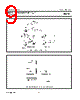
6 / 25 page  December 1992 6 Philips Semiconductors Product specification PAL/NTSC/SECAM decoder/sync processor TDA9141 FUNCTIONAL DESCRIPTION General The TDA9141 is an I2C-bus controlled, alignment-free PAL/NTSC/SECAM colour decoder/sync processor which has been designed for use with baseband chrominance delay lines. In the standard operating mode the I2C-bus address is 8A. If the address input is connected to the positive rail the address will change to 8E. Input switch WARNING: THE VOLTAGE ON THE CHROMINANCE PIN MUST NEVER EXCEED 5.5 V. IF IT DOES THE IC ENTERS A TEST MODE . The TDA9141 has a two pin input for CVBS or YC signals which can be selected via the I2C-bus. The input selector also has a position in which it automatically detects whether a CVBS or YC signal is on the input. In this input selector position, standard identification first takes place on an added Y/CVBS and C input signal. After that, both chrominance signal input amplitudes are checked once and the input with the strongest chrominance burst signal is selected. The input switch status is read out by the I2C-bus via output bit YC. CVBS output In the standard operating mode with the I2C-bus address 8A, a CVBS output signal is available on the address pin, which represents either the CVBS input signal or the Y/C input signal, added into a CVBS signal RGB colour matrix WARNING: THE VOLTAGE ON THE UIN PIN MUST NEVER EXCEED 5.5 V. IFIT DOES THE IC ENTERS A TEST MODE. The TDA9141 has a colour matrix to convert RGB input signals into YUV signals. A fast switch, controlled by the signal on pin F and enabled by the I2C-bus via EFS (enable fast switch), can select between these YUV signals and the YUV signals of the decoder. The Y signal is internally connected to the switch. The −(R−Y) and −(B−Y) output signals of the decoder have to first be delayed in external baseband chrominance delay lines. The outputs of the delay lines must be connected to the UV input pins. If the RGB signals are not synchronous with the selected decoder input signal, clamping of the RGB input signals is possible by I2C-bus selection of STM (search tuning mode), EFS and by feeding an external clamping signal to the CLP pin. Also in search tuning mode the VA output will be in a high impedance OFF-state. Standard identification The standards which the TDA9141 can decode are dependent on the choice of external crystals. If a 4.4 MHz and a 3.6 MHz crystal are used then SECAM, PAL 4.4/3.6 and NTSC 4.4/3.6 can be decoded. If two 3.6 MHz crystals are used then only PAL 3.6 and NTSC 3.6 can be decoded. Which 3.6 MHz standards can be decoded is dependent on the exact frequencies of the 3.6 MHz crystals. In an application where not all standards are required only one crystal is sufficient (in this instance the crystal must be connected to the reference crystal input (pin 30)). If a 4.4 MHz crystal is used it must always be connected to pin 30. Both crystals are used to provide a reference for the filters and the horizontal PLL, however, only the reference crystal is used to provide a reference for the SECAM demodulator. To enable the calibrating circuits to be adjusted exactly two bits from I2C-bus subaddress 00 are used to indicate which crystals are connected to the IC. The standard identification circuit is a digital circuit without external components; the search loop is illustrated in Fig.3. The decoder (via the I2C-bus) can be forced to decode either SECAM or PAL/NTSC (but not PAL or NTSC). Crystal selection can also be forced. Information concerning which standard and which crystal have been selected and whether the colour killer is ON or OFF is provided by the read out. Using the forced-mode does not affect the search loop, it does, however, prevent the decoder from reaching or staying in an unwanted state. The identification circuit skips impossible standards (e.g. SECAM when no 4.4 MHz crystal is fitted) and illegal standards (e.g. is forced mode). To reduce the risk of wrong identification PAL has priority over SECAM (only line identification is used for SECAM). Integrated filters All filters, including the luminance delay line, are an integral part of the IC. The filters are gyrator-capacitor type filters. The resonant frequency of the filters is controlled by a circuit that uses the active crystal to tune the SECAM Cloche filter during the vertical flyback time. The remaining filters and the luminance delay line are matched to this filter. The filters can be switched to either 4.43 MHz, 4.28 MHz or 3.58 MHz irrespective of the frequency of the active crystal. The switching is controlled by the identification circuit. In YC mode the chrominance notch filter is bypassed, to preserve full signal bandwidth. For a CVBS signal the chrominance notch filter can be bypassed by I2C-bus selection of TB (trap bypass). The luminance delay line delivers the Y signal to the output 60 ns after the −(R−Y) and −(B−Y) signals have arrived at their outputs. |
|
|
Link URL |
| Cho đến nay ALLDATASHEET có giúp ích cho doanh nghiệp của bạn hay không? [ DONATE ] |
Alldatasheet là | Quảng cáo | Liên lạc với chúng tôi | Chính sách bảo mật | Liên kết đến bảng dữ liệu | Trao đổi link | Tìm kiếm theo nhà sản xuất All Rights Reserved©Alldatasheet.com |
| Russian : Alldatasheetru.com | Korean : Alldatasheet.co.kr | Spanish : Alldatasheet.es | French : Alldatasheet.fr | Italian : Alldatasheetit.com Portuguese : Alldatasheetpt.com | Polish : Alldatasheet.pl | Vietnamese : Alldatasheet.vn Indian : Alldatasheet.in | Mexican : Alldatasheet.com.mx | British : Alldatasheet.co.uk | New Zealand : Alldatasheet.co.nz |
|
Family Site : ic2ic.com |
icmetro.com |
 Vietnamese ▼
 English
 Chinese
 German
 Japanese
 Russian
 Korean
 Spanish
 French
 Italian
 Portuguese
 Polish
 Vietnamese
 Indian
 Mexican
 British
 New Zealand