|
công cụ tìm kiếm bảng dữ liệu linh kiện điện tử |
|
|
công cụ tìm kiếm bảng dữ liệu linh kiện điện tử |
|
CCG3PA bảng dữ liệu(PDF) 7 Page - Cypress Semiconductor |
|
|
|||||||||||||||||||||||||||||
CCG3PA bảng dữ liệu(HTML) 7 Page - Cypress Semiconductor |
|
|
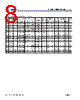
7 / 37 page  Document Number: 002-16951 Rev. *F Page 7 of 37 EZ-PD™ CCG3PA Datasheet Pinouts Table 2. CCG3PA Pin Descriptions 24-Pin QFN 16-Pin SOIC Pin Name Description 1 – P1.0 Port 1 pin 0: GPIO/UART_1_CTS/I2C_SDA_1[1] / TCPWM_line_0[2], Programmable SCP/OCP/OVP/UVP Fault indication 2 – P1.1 Port 1 pin 1: GPIO/UART_1_RTS/I2C_SCL_1[1] / TCPWM_line_1[3], Programmable SCP/OCP/OVP/UVP Fault indication 3 5 VBUS_P_CTRL Provider (PMOS) FET control (30-V Tolerant) 0: Path ON 1: Path OFF 4 – VBUS_C_CTRL VBUS Consumer (PMOS) FET Control (30-V Tolerant) 0: Path ON Z: Path OFF 5 – DP1/P1.2 USB D+/Port 1 pin 2: GPIO/UART_1_TX1/AFC/QC/BC 1.2/Apple Charging/No IEC 6 – DM1/P1.3 USB D-/Port 1 pin 3: GPIO/UART_1_RX1/AFC/QC/BC 1.2/Apple Charging/No IEC 7 6 SWD_DAT_0/P0.0 Port 0 pin 0: GPIO/OVT/I2C_SDA_0/TCPWM_line_0/UART_0_CTS 8 7 SWD_CLK_0/P0.1 Port 0 pin 1: GPIO/OVT/I2C_SCL_0/TCPWM_line_1/UART_0_RTS 9 8 AXRES/P2.0 Port 2 pin 0: GPIO/Alternate XRES[4]/TCPWM_line_0//UART_0_TX0 10 – P2.1 Port 2 pin 1: GPIO/TCPWM_line_1//UART_0_RX0 11 9 VBUS_C_MON_DIS- CHARGE Type C VBUS Monitor with Internal Discharge FET 12 – P2.2 Port 2 pin 2: GPIO with Open drain with pull-up assist. Configurable as GPIO_20VT/I2C_SDA_1/IEC. Tolerant to temporary short to VBUS pin.. 13 – P2.3 Port 2 pin 3: GPIO with Open drain with pull-up assist. Configurable as GPIO_20VT/I2C_SCL_1/IEC. Tolerant to temporary short to VBUS pin. 14 10 CC2 Communication Channel 2 with Dead-battery Rd Bonding Option/IEC. Tolerant to temporary short to VBUS pin. 15 11 CC1 Communication Channel 1 with Dead-battery Rd Bonding Option/IEC. Tolerant to temporary short to VBUS pin. 16 12 DM0/P3.1 USB D-/Port 3 pin 1: GPIO/UART_1_RX0/AFC/QC/BC 1.2/Apple Charging/IEC 17 13 DP0/P3.0 USB D+/Port 3 pin 0: GPIO/UART_1_TX0/AFC/QC/BC 1.2/Apple Charging/IEC 18 14 VBUS_IN_DIS CHARGE VBUS Power IN (3.0 V–24.5 V) with Internal Discharge FET 19 16 CSP CS +: Current sense input 20 1 FB Voltage regulation feedback pin 21 2 CATH/COMP Cathode of voltage regulation and compensation for other applications 22 15 GND Ground 23 3 VDDD Power Input: 2.7 V–5.5 V 24 4 VCCD 1.8-V Core Voltage pin (not intended for use as a power source) – – EPAD Ground Note 1. Out of the two SCB blocks (SCB0 and SCB1), while the SCB0’s I2C functionality is mapped out to the P0.0/P0.1 GPIO pins, the I2C functionality of SCB1 provides flexibility to have it mapped either on P1.0/P1.1 OR P2.2/P2.3 GPIO pins. 2. TCPWM_line_0 can be mapped to port pins P1.0, P0.0, P2.0 or P2.2. 3. TCPWM_line_1 can be mapped to port pins P1.1, P0.1, P2.1 or P2.3. 4. AXRES pin will be internally pulled up during the Power On I/O initialization time (see Table 6 for more details). 5. See Table 9 and Table 10 for specifications related to these pins. |
|
Link URL |
| Cho đến nay ALLDATASHEET có giúp ích cho doanh nghiệp của bạn hay không? [ DONATE ] |
Alldatasheet là | Quảng cáo | Liên lạc với chúng tôi | Chính sách bảo mật | Liên kết đến bảng dữ liệu | Trao đổi link | Tìm kiếm theo nhà sản xuất All Rights Reserved©Alldatasheet.com |
| Russian : Alldatasheetru.com | Korean : Alldatasheet.co.kr | Spanish : Alldatasheet.es | French : Alldatasheet.fr | Italian : Alldatasheetit.com Portuguese : Alldatasheetpt.com | Polish : Alldatasheet.pl | Vietnamese : Alldatasheet.vn Indian : Alldatasheet.in | Mexican : Alldatasheet.com.mx | British : Alldatasheet.co.uk | New Zealand : Alldatasheet.co.nz |
|
Family Site : ic2ic.com |
icmetro.com |
 Vietnamese ▼
 English
 Chinese
 German
 Japanese
 Russian
 Korean
 Spanish
 French
 Italian
 Portuguese
 Polish
 Vietnamese
 Indian
 Mexican
 British
 New Zealand