|
công cụ tìm kiếm bảng dữ liệu linh kiện điện tử |
|
|
công cụ tìm kiếm bảng dữ liệu linh kiện điện tử |
|
AP3015 bảng dữ liệu(PDF) 8 Page - BCD Semiconductor Manufacturing Limited |
|
|
|||||||||||||||||||||||||||||
AP3015 bảng dữ liệu(HTML) 8 Page - BCD Semiconductor Manufacturing Limited |
|
|
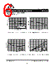
8 / 11 page  MICRO POWER STEP-UP DC-DC CONVERTER AP3015/A 8 Aug. 2006 Rev. 1. 0 BCD Semiconductor Manufacturing Limited Preliminary Datasheet Figure 13. Efficiency Typical Performance Characteristics (Continued) Figure 12. Efficiency Unless otherwise noted, VIN=1.2V Application Information Operating Principles AP3015/A feature a constant off-time control scheme. Refer to Figure 3,the bandgap voltage VREF (1.23V typical) is used to control the output voltage. When the voltage at the FB pin drops below the lower hysteresis point of Feedback Comparator (typical hysteresis is 8mV), the Feedback Comparator enables the chip and the NPN power switch is turned on, the current in the inductor begins to ramp up and store energy in the coil while the load current is supplied by the output capacitor. Once the current in the inductor reaches the current limit, the Current-Limit Comparator resets the 400ns One-Shot which turns off the NPN switch for 400ns. The SW voltage rises to the output voltage plus a diode drop and the inductor current begins to ramp down. During this time the energy stored in the inductor is transferred to COUT and the load. After the 400ns off-time, the NPN switch is turned on and energy will be stored in the inductor again. This cycle will continue until the voltage at FB pin reaches 1.23V, the Feedback Comparator disables the chip and turns off the NPN switch. The load current is then supplied solely by output capacitor and the output voltage will decrease. When the FB pin voltage drops below the lower hysteresis point of Feedback Comparator, the Feedback Comparator enables the device and repeats the cycle described previously. Under not switching condition, the IQ of the device is about 17 µA. The AP3015/A contain additional circuitry to provide protection during start-up or under short-circuit conditions. When the FB pin voltage is lower than approximately 0.6V, the switch off-time is increased to 1.5 µs and the current limit is reduced to about 250mA (70mA for AP3015A). This reduces the average inductor current and helps to minimize the power dissipation in the AP3015/A power switch, in the external inductor and in the diode. The SHDN pin can be used to turn off the AP3015/A and reduce the IQ to less than 1µA. In shutdown mode the output voltage will be a diode drop below the input voltage. 0.1 1 10 50 55 60 65 70 75 80 85 Load Current (mA) AP3015 V OUT =20V, L=10µH, C OUT =1µF Refer to Figure 14 V IN =4.2V V IN =3.3V V IN =2.5V 0.1 1 10 50 55 60 65 70 75 80 85 Load Current (mA) AP3015A V OUT =3.3V, L=10µH, C OUT =20µF Refer to Figure 15 V IN =2.5V V IN =1.2V |
|
|
Link URL |
| Cho đến nay ALLDATASHEET có giúp ích cho doanh nghiệp của bạn hay không? [ DONATE ] |
Alldatasheet là | Quảng cáo | Liên lạc với chúng tôi | Chính sách bảo mật | Liên kết đến bảng dữ liệu | Trao đổi link | Tìm kiếm theo nhà sản xuất All Rights Reserved©Alldatasheet.com |
| Russian : Alldatasheetru.com | Korean : Alldatasheet.co.kr | Spanish : Alldatasheet.es | French : Alldatasheet.fr | Italian : Alldatasheetit.com Portuguese : Alldatasheetpt.com | Polish : Alldatasheet.pl | Vietnamese : Alldatasheet.vn Indian : Alldatasheet.in | Mexican : Alldatasheet.com.mx | British : Alldatasheet.co.uk | New Zealand : Alldatasheet.co.nz |
|
Family Site : ic2ic.com |
icmetro.com |
 Vietnamese ▼
 English
 Chinese
 German
 Japanese
 Russian
 Korean
 Spanish
 French
 Italian
 Portuguese
 Polish
 Vietnamese
 Indian
 Mexican
 British
 New Zealand