|
công cụ tìm kiếm bảng dữ liệu linh kiện điện tử |
|
|
công cụ tìm kiếm bảng dữ liệu linh kiện điện tử |
|
ADF4252BCPZ-R7 bảng dữ liệu(PDF) 14 Page - Analog Devices |
|
|
|||||||||||||||||||||||||||||
ADF4252BCPZ-R7 bảng dữ liệu(HTML) 14 Page - Analog Devices |
|
|
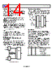
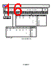
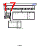
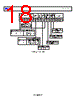
14 / 30 page  ADF4252 Data Sheet Rev. E | Page 14 of 30 IF PRESCALER (P/P + 1) The dual modulus IF prescaler (P/P + 1), along with the IF A and B counters, enables the large division ratio, N, to be realized (N = PB + A). Operating at CML levels, the prescaler takes the clock from the IF input stage and divides it down to a manageable frequency for the CMOS IF A and B counters. IF A AND B COUNTERS The IF A and B CMOS counters combine with the dual modulus IF prescaler to allow a wide ranging division ratio in the PLL feedback counter. The counters are guaranteed to work when the prescaler output is 150 MHz or less. PULSE SWALLOW FUNCTION The IF A and B counters, in conjunction with the dual modulus IF prescaler, make it possible to generate output frequencies that are spaced only by the reference frequency divided by R. See the Device Programming after Initial Power-Up section for examples. The equation for the IF VCO (IFOUT) frequency is PFD OUT f A B P IF ] ) [( (3) where: IFOUT is the output frequency of the external VCO. P is the preset modulus of IF dual modulus prescaler. B is the preset divide ratio of the binary 12-bit counter (3 to 4095). A is the preset divide ratio of the binary 6-bit swallow counter (0 to 63). fPFD is obtained using Equation 2. PHASE FREQUENCY DETECTOR (PFD) AND CHARGE PUMP The PFD takes inputs from the R counter and N counter and produces an output proportional to the phase and frequency difference between them. Figure 32 is a simplified schematic. The antibacklash pulse ensures that there is no dead zone in the PFD transfer function and minimizes phase noise and reference spurs. +IN D1 Q1 CLR1 U1 U3 DELAY ELEMENT HI UP D2 Q2 CLR2 U2 HI DOWN CHARGE PUMP CP –IN Figure 32. PFD Simplified Schematic MUXOUT AND LOCK DETECT The output multiplexer on the ADF4252 allows the user to access various internal points on the chip. The state of MUXOUT is controlled by M4, M3, M2, and M1 in the master register. Table 5 shows the full truth table. Figure 33 shows the MUXOUT section in block diagram format. LOGIC LOW IF ANALOG LOCK DETECT IF R DIVIDER OUTPUT IF N DIVIDER OUTPUT RF ANALOG LOCK DETECT IF/RF ANALOG LOCK DETECT IF DIGITAL LOCK DETECT LOGIC HIGH RF R DIVIDER OUTPUT RF N DIVIDER OUTPUT THREE-STATE OUTPUT RF DIGITAL LOCK DETECT RF/IF DIGITAL LOCK DETECT LOGIC HIGH LOGIC LOW MUX CONTROL MUXOUT DVDD DGND Figure 33. MUXOUT Circuit LOCK DETECT MUXOUT can be programmed for two types of lock detect: digital and analog. Digital is active high. The N-channel open- drain analog lock detect must be operated with an external pull- up resistor of 10 kΩ nominal. When lock has been detected, this output is high with narrow low going pulses. INPUT SHIFT REGISTER Data is clocked in on each rising edge of CLK. The data is clocked in MSB first. Data is transferred from the input register to one of seven latches on the rising edge of LE. The destination latch is determined by the state of the three control bits (C2, C1, and C0) in the shift register. These are the three LSBs: DB2, DB1, and DB0, as shown in Figure 2. The truth table for these bits is shown in Table 5. Figure 34 summarizes how the registers are programmed. Table 5. Control Bit Truth Table C2 C1 C0 Data Latch 0 0 0 RF N divider register 0 0 1 RF R divider register 0 1 0 RF control register 0 1 1 Master register 1 0 0 IF N divider register 1 0 1 IF R divider register 1 1 0 IF control register |
|
Link URL |
| Cho đến nay ALLDATASHEET có giúp ích cho doanh nghiệp của bạn hay không? [ DONATE ] |
Alldatasheet là | Quảng cáo | Liên lạc với chúng tôi | Chính sách bảo mật | Liên kết đến bảng dữ liệu | Trao đổi link | Tìm kiếm theo nhà sản xuất All Rights Reserved©Alldatasheet.com |
| Russian : Alldatasheetru.com | Korean : Alldatasheet.co.kr | Spanish : Alldatasheet.es | French : Alldatasheet.fr | Italian : Alldatasheetit.com Portuguese : Alldatasheetpt.com | Polish : Alldatasheet.pl | Vietnamese : Alldatasheet.vn Indian : Alldatasheet.in | Mexican : Alldatasheet.com.mx | British : Alldatasheet.co.uk | New Zealand : Alldatasheet.co.nz |
|
Family Site : ic2ic.com |
icmetro.com |
 Vietnamese ▼
 English
 Chinese
 German
 Japanese
 Russian
 Korean
 Spanish
 French
 Italian
 Portuguese
 Polish
 Vietnamese
 Indian
 Mexican
 British
 New Zealand