|
công cụ tìm kiếm bảng dữ liệu linh kiện điện tử |
|
|
công cụ tìm kiếm bảng dữ liệu linh kiện điện tử |
|
ADF4252BCPZ-R7 bảng dữ liệu(PDF) 7 Page - Analog Devices |
|
|
|||||||||||||||||||||||||||||
ADF4252BCPZ-R7 bảng dữ liệu(HTML) 7 Page - Analog Devices |
|
|
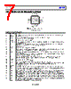
7 / 30 page  Data Sheet ADF4252 Rev. E | Page 7 of 30 PIN CONFIGURATION AND FUNCTION DESCRIPTIONS 18 CPGND2 NOTES 1. THE EXPOSED PAD MUST BE CONNECTED TO AGND. 17 DVDD 16 IFINA 15 IFINB 14 AGND2 13 RSET CPRF 1 CPGND1 2 RFINA 3 RFINB 4 AGND1 5 MUXOUT 6 ADF4252 TOP VIEW Figure 3. Pin Configuration Table 4. Pin Function Descriptions Pin No. Mnemonic Function 1 CPRF RF Charge Pump Output. This pin is normally connected to a loop filter that drives the input to an external VCO. 2 CPGND1 RF Charge Pump Ground. 3 RFINA Input to the RF Prescaler. This small signal input is normally taken from the VCO. 4 RFINB Complementary Input to the RF Prescaler. 5 AGND1 Analog Ground for the RF Synthesizer. 6 MUXOUT This multiplexer output allows either the RF or IF lock detect, the scaled RF or IF, or the scaled reference frequency to be accessed externally. 7 REFIN Reference Input. This pin is a CMOS input with a nominal threshold of VDD/2 and an equivalent input resistance of 100 kΩ. This input can be driven from a TTL or CMOS crystal oscillator. 8 REFOUT Reference Output. 9 DGND Digital Ground for the Fractional Interpolator. 10 CLK Serial Clock Input. This serial clock is used to clock in the serial data to the registers. The data is latched into the shift register on the CLK rising edge. This input is a high impedance CMOS input. 11 DATA Serial Data Input. The serial data is loaded MSB first with the three LSBs being the control bits. This input is a high impedance CMOS input. 12 LE Load Enable, CMOS Input. When LE goes high, the data stored in the shift registers is loaded into one of the seven latches, the latch being selected using the control bits. 13 RSET Connecting a resistor between this pin and ground sets the minimum charge pump output current. The relationship between ICP and RSET is ICP_MIN = 1.6875/RSET. Therefore, with RSET = 2.7 kΩ, ICP_MIN = 0.625 mA. 14 AGND2 Ground for the IF Synthesizer. 15 IFINB Complementary Input to the IF Prescaler. 16 IFINA Input to the IF Prescaler. This small signal input is normally taken from the IF VCO. 17 DVDD Positive Power Supply for the Fractional Interpolator Section. Decoupling capacitors to the ground plane must be placed as close as possible to this pin. DVDD must have the same voltage as VDD1, VDD2, and VDD3. 18 CPGND2 IF Charge Pump Ground. 19 CPIF IF Charge Pump Output. This pin is normally connected to a loop filter that drives the input to an external VCO. 20 VP2 IF Charge Pump Power Supply. Decoupling capacitors to the ground plane must be placed as close as possible to this pin. This voltage must be greater than or equal to VDD2. 21 VDD2 Positive Power Supply for the IF Section. Decoupling capacitors to the ground plane must be placed as close as possible to this pin. VDD2 has a value 3 V ± 10%. VDD2 must have the same voltage as VDD1, VDD3, and DVDD. 22 VDD3 Positive Power Supply for the RF Digital Section. Decoupling capacitors to the ground plane must be placed as close as possible to this pin. VDD3 has a value 3 V ± 10%. VDD3 must have the same voltage as VDD1, VDD2, and DVDD. 23 VDD1 Positive Power Supply for the RF Analog Section. Decoupling capacitors to the ground plane must be placed as close as possible to this pin. VDD1 has a value 3 V ± 10%. VDD1 must have the same voltage as VDD2, VDD3, and DVDD. 24 VP1 RF Charge Pump Power Supply. Decoupling capacitors to the ground plane must be placed as close as possible to this pin. This voltage must be greater than or equal to VDD1. EPAD Exposed Pad. The exposed pad must be connected to AGND. |
|
Link URL |
| Cho đến nay ALLDATASHEET có giúp ích cho doanh nghiệp của bạn hay không? [ DONATE ] |
Alldatasheet là | Quảng cáo | Liên lạc với chúng tôi | Chính sách bảo mật | Liên kết đến bảng dữ liệu | Trao đổi link | Tìm kiếm theo nhà sản xuất All Rights Reserved©Alldatasheet.com |
| Russian : Alldatasheetru.com | Korean : Alldatasheet.co.kr | Spanish : Alldatasheet.es | French : Alldatasheet.fr | Italian : Alldatasheetit.com Portuguese : Alldatasheetpt.com | Polish : Alldatasheet.pl | Vietnamese : Alldatasheet.vn Indian : Alldatasheet.in | Mexican : Alldatasheet.com.mx | British : Alldatasheet.co.uk | New Zealand : Alldatasheet.co.nz |
|
Family Site : ic2ic.com |
icmetro.com |
 Vietnamese ▼
 English
 Chinese
 German
 Japanese
 Russian
 Korean
 Spanish
 French
 Italian
 Portuguese
 Polish
 Vietnamese
 Indian
 Mexican
 British
 New Zealand