|
công cụ tìm kiếm bảng dữ liệu linh kiện điện tử |
|
|
công cụ tìm kiếm bảng dữ liệu linh kiện điện tử |
|
MIC2194 bảng dữ liệu(PDF) 7 Page - Micrel Semiconductor |
|
|
|||||||||||||||||||||||||||||
MIC2194 bảng dữ liệu(HTML) 7 Page - Micrel Semiconductor |
|
|
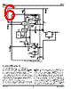
7 / 10 page  October 2002 7 MIC2194 MIC2194 Micrel The MIC2194 controller is broken down into several func- tions. • Control loop • PWM operation • Current mode control • Current limit • Reference, enable and UVLO • MOSFET gate drive • Oscillator Control Loop PWM Control Loop The MIC2194 uses current mode control to regulate the output voltage. This dual control loop method (illustrated in Figure 2) senses the output voltage (outer loop) and the inductor current (inner loop). It uses inductor current and output voltage to determine the duty cycle of the buck converter. Sampling the inductor current effectively removes the inductor from the control loop, which simplifies compen- sation. Switching Converter Voltage Divider VREF VERROR VERROR tON tPER D = tON/tPER IINDUCTOR IINDUCTOR Switch Driver VOUT VIN Figure 2. Current Mode Control Example As shown in Figure 1, the inductor current is sensed by measuring the voltage across the resistor, R SENSE. A ramp is added to the amplified current sense signal to provide slope compensation, which is required to prevent unstable opera- tion at duty cycles greater than 50%. A transconductance amplifier is used for the error amplifier, which compares an attenuated sample of the output voltage with a reference voltage. The output of the error amplifier is the compensation pin (COMP), which is compared to the current sense waveform in the PWM block. When the current signal becomes greater than the error signal, the comparator turns off the high side drive. The COMP pin provides access to the output of the error amplifier and allows the use of external components to stabilize the voltage loop. Current Limit The output current is detected by the voltage drop across the external current sense resistor (R SENSE in Figure 1.). The current sense resistor must be sized using the minimum current limit threshold. The external components must be designed to withstand the maximum current limit. The current sense resistor value is calculated by the equation below: R MIN CURRENT SENSE THRESHOLD I SENSE OUT MAX = __ _ _ The maximum output current is: I MAX CURRENT SENSE THRESHOLD R OUT MAX SENSE _ __ _ = The current sense pins VIN (pin 8) and CSL (pin 4) are noise sensitive due to the low signal level, high input impedance and input ripple voltage. The PCB traces should be short and routed close to each other. A 0.1 µF capacitor across the pins will attenuate high frequency switching noise. When the peak inductor current exceeds the current limit threshold, the overcurrent comparator turns off the high-side MOSFET for the remainder of the switching cycle, effectively decreasing the duty cycle. The output voltage drops as additional load current is pulled from the converter. When the voltage at the feedback pin (FB) reaches approximately 0.3V, the circuit enters frequency foldback mode and the oscillator frequency will drop to 1/4 of the switching frequency. This limits the maximum output power delivered to the load under a short circuit condition. Reference, Enable and UVLO Circuits The output drivers are enabled when the following conditions are satisfied: • The V DD voltage (pin 5) is greater than its undervoltage threshold. • The voltage on the enable pin (pin 3) is greater than the enable UVLO threshold. The enable pin (pin 3) has two threshold levels, allowing the MIC2194 to shut down in a low current mode, or turn off output switching in standby mode. An enable pin voltage lower than the shutdown threshold turns off all the internal circuitry and places the MIC2194 in a micropower shutdown mode. If the enable pin voltage is between the shutdown and standby thresholds, the internal bias, V DD and reference voltages are turned on. The output drivers are inhibited from switching. The OUTP pin is in a high state. Raising the enable voltage above the standby threshold enables the output driver. The standby threshold is specified in the electrical characteristics. A resistor divider can be used with the enable pin to prevent the power supply from turning on until a specified input voltage is reached. The circuit in Figure 3 shows how to connect the resistors. |
|
|
Link URL |
| Cho đến nay ALLDATASHEET có giúp ích cho doanh nghiệp của bạn hay không? [ DONATE ] |
Alldatasheet là | Quảng cáo | Liên lạc với chúng tôi | Chính sách bảo mật | Liên kết đến bảng dữ liệu | Trao đổi link | Tìm kiếm theo nhà sản xuất All Rights Reserved©Alldatasheet.com |
| Russian : Alldatasheetru.com | Korean : Alldatasheet.co.kr | Spanish : Alldatasheet.es | French : Alldatasheet.fr | Italian : Alldatasheetit.com Portuguese : Alldatasheetpt.com | Polish : Alldatasheet.pl | Vietnamese : Alldatasheet.vn Indian : Alldatasheet.in | Mexican : Alldatasheet.com.mx | British : Alldatasheet.co.uk | New Zealand : Alldatasheet.co.nz |
|
Family Site : ic2ic.com |
icmetro.com |
 Vietnamese ▼
 English
 Chinese
 German
 Japanese
 Russian
 Korean
 Spanish
 French
 Italian
 Portuguese
 Polish
 Vietnamese
 Indian
 Mexican
 British
 New Zealand