|
công cụ tìm kiếm bảng dữ liệu linh kiện điện tử |
|
|
công cụ tìm kiếm bảng dữ liệu linh kiện điện tử |
|
AT86RF211DAI-R bảng dữ liệu(PDF) 23 Page - ATMEL Corporation |
|
|
|||||||||||||||||||||||||||||
AT86RF211DAI-R bảng dữ liệu(HTML) 23 Page - ATMEL Corporation |
|
|
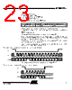
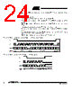
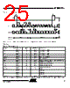
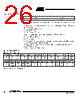
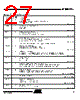
23 / 48 page  23 AT86RF211 1942C–WIRE–06/02 • Register Interface Format A message is made of 3 fields: – address A[3:0]: 4 bits (MSB first) – R/W: read/write selection – data D[31:0]: up to 32 bits (MSB first) Variable register length and partial read or write cycles are supported. In case of partial read or write cycles, the first data (in or out) is always the MSB of the register. • WRITE Mode (R/W = 1) The address, R/W and data bits are clocked on the rising edge of SCK. If the number of data bits is lower than the register capacity, the LSB bits keep their former value allowing safe partial write. If the number of data bits is greater than the reg- ister capacity, the extra bits are ignored. The data is actually written into the register on the rising edge of SLE when the data length is less or equal to the register length. When trying to write more data than the register length, data field is written on the first extra rising clock edge regarding register length. Figure 29. Write Chronogram: Complete Write Cycle in a 10 bits Register The complete register of 10 bits is updated on a rising edge of SLE. Figure 30. Write Chronogram: Partial Write Cycle, Writing 2 bits ADDRESS R/W DATA up to 32 bits (variable length) A[3] A[2] A[1] A[0] R/W MSB D[nbit-1:0] LSB D[8] A[1] A[2] D[7] A[3] R / W SLE SCK SDATA D[6] D[5] D[4] D[3] D[2] D[1] D[0] A[0] D[9] A[1] A[2] A[3] R/W SLE SCK SDATA D[30] A[0] D[31] |
|
Link URL |
| Cho đến nay ALLDATASHEET có giúp ích cho doanh nghiệp của bạn hay không? [ DONATE ] |
Alldatasheet là | Quảng cáo | Liên lạc với chúng tôi | Chính sách bảo mật | Liên kết đến bảng dữ liệu | Trao đổi link | Tìm kiếm theo nhà sản xuất All Rights Reserved©Alldatasheet.com |
| Russian : Alldatasheetru.com | Korean : Alldatasheet.co.kr | Spanish : Alldatasheet.es | French : Alldatasheet.fr | Italian : Alldatasheetit.com Portuguese : Alldatasheetpt.com | Polish : Alldatasheet.pl | Vietnamese : Alldatasheet.vn Indian : Alldatasheet.in | Mexican : Alldatasheet.com.mx | British : Alldatasheet.co.uk | New Zealand : Alldatasheet.co.nz |
|
Family Site : ic2ic.com |
icmetro.com |
 Vietnamese ▼
 English
 Chinese
 German
 Japanese
 Russian
 Korean
 Spanish
 French
 Italian
 Portuguese
 Polish
 Vietnamese
 Indian
 Mexican
 British
 New Zealand