|
công cụ tìm kiếm bảng dữ liệu linh kiện điện tử |
|
|
công cụ tìm kiếm bảng dữ liệu linh kiện điện tử |
|
ADP1290ACBZ-R7 bảng dữ liệu(PDF) 9 Page - Analog Devices |
|
|
|||||||||||||||||||||||||||||
ADP1290ACBZ-R7 bảng dữ liệu(HTML) 9 Page - Analog Devices |
|
|
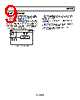
9 / 12 page  Data Sheet ADP1290 THEORY OF OPERATION The ADP1290 is a high-side NMOS load switch, controlled by an internal charge pump. The ADP1290 is designed to operate with power supply voltages between 2.3 V and 13.2 V. An internal charge pump biases the NMOS switch to achieve a relatively constant, ultralow on resistance of 40 mΩ across the entire input voltage range. The use of the internal charge pump also allows controlled turn on times. Turning the NMOS switch on and off is controlled by the enable input, EN, which is capable of interfacing directly with 1.2 V logic signals. GND EN VIN VOUT CHARGE PUMP AND SLEW RATE CONTROL Figure 20. Functional Block Diagram The ADP1290 is capable of 2 A of continuous current as long as TJ is less than 85°C. Between 85°C and 105°C, the rated current decreases linearly to 1.6 A. ESD protection structures are shown in the block diagram as Zener diodes. The ADP1290 is a low quiescent current device with a weak 15 nA pull-down current sink on its enable pin (EN). The ADP1290 is available in a space-saving 1.0 mm × 1.5 mm, 0.5 mm pitch, 6-ball WLCSP. Rev. 0 | Page 9 of 12 |
|
|
Link URL |
| Cho đến nay ALLDATASHEET có giúp ích cho doanh nghiệp của bạn hay không? [ DONATE ] |
Alldatasheet là | Quảng cáo | Liên lạc với chúng tôi | Chính sách bảo mật | Liên kết đến bảng dữ liệu | Trao đổi link | Tìm kiếm theo nhà sản xuất All Rights Reserved©Alldatasheet.com |
| Russian : Alldatasheetru.com | Korean : Alldatasheet.co.kr | Spanish : Alldatasheet.es | French : Alldatasheet.fr | Italian : Alldatasheetit.com Portuguese : Alldatasheetpt.com | Polish : Alldatasheet.pl | Vietnamese : Alldatasheet.vn Indian : Alldatasheet.in | Mexican : Alldatasheet.com.mx | British : Alldatasheet.co.uk | New Zealand : Alldatasheet.co.nz |
|
Family Site : ic2ic.com |
icmetro.com |
 Vietnamese ▼
 English
 Chinese
 German
 Japanese
 Russian
 Korean
 Spanish
 French
 Italian
 Portuguese
 Polish
 Vietnamese
 Indian
 Mexican
 British
 New Zealand