|
công cụ tìm kiếm bảng dữ liệu linh kiện điện tử |
|
|
công cụ tìm kiếm bảng dữ liệu linh kiện điện tử |
|
LEDV3 bảng dữ liệu(PDF) 15 Page - Midas Components |
|
|
|||||||||||||||||||||||||||||
LEDV3 bảng dữ liệu(HTML) 15 Page - Midas Components |
|
|
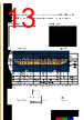
15 / 21 page  9.Interface timing 9.1. INPUT SIGNAL TIMING SPECIFICATIONS The input signal timing specifications are shown as the following table and timing diagram. Signal Item Symbol Min. Typ. Max. Unit Note LVDS Clock Frequency Fc 53.35 65 80 MHz - Period Tc 12.5 15.38 18.75 ns Input cycle to cycle jitter Trcl --- --- 200 ns (a) Input Clock to data skewTLVCCS -0.02*Tc - 0.02*Tc ps (b) Spread spectrum modulation range Fclkin_mod - - 1.02*Fc MHz (c) Spread spectrum modulation frequency FSSM - - 200 KHz Vertical Display Term Frame Rate Fr -- 60 -- Hz Tv=Tvd+Tvb Total Tv 780 806 1200 Th - Active Display Tvd 768 768 768 Th - Blank Tvb Tv-Tvd 38 Tv-Tvd Th - Horizontal Display Term Total Th 1140 1344 1600 Tc Th=Thd+Thb Active Display Thd 1024 1024 1024 Tc - Blank Thb Th-Thd 320 Th-Thd Tc - Note (1) Because this module is operated by DE only mode, Hsync and Vsync input signals should be set to low logic level or ground. Otherwise, this module would operate abnormally. Note (2) The Tv(Tvd+Tvb) must be integer, otherwise, the module would operate abnormally. INPUT SIGNAL TIMING DIAGRAM Page 15 of 21 |
|
|
Link URL |
| Cho đến nay ALLDATASHEET có giúp ích cho doanh nghiệp của bạn hay không? [ DONATE ] |
Alldatasheet là | Quảng cáo | Liên lạc với chúng tôi | Chính sách bảo mật | Liên kết đến bảng dữ liệu | Trao đổi link | Tìm kiếm theo nhà sản xuất All Rights Reserved©Alldatasheet.com |
| Russian : Alldatasheetru.com | Korean : Alldatasheet.co.kr | Spanish : Alldatasheet.es | French : Alldatasheet.fr | Italian : Alldatasheetit.com Portuguese : Alldatasheetpt.com | Polish : Alldatasheet.pl | Vietnamese : Alldatasheet.vn Indian : Alldatasheet.in | Mexican : Alldatasheet.com.mx | British : Alldatasheet.co.uk | New Zealand : Alldatasheet.co.nz |
|
Family Site : ic2ic.com |
icmetro.com |
 Vietnamese ▼
 English
 Chinese
 German
 Japanese
 Russian
 Korean
 Spanish
 French
 Italian
 Portuguese
 Polish
 Vietnamese
 Indian
 Mexican
 British
 New Zealand