|
công cụ tìm kiếm bảng dữ liệu linh kiện điện tử |
|
|
công cụ tìm kiếm bảng dữ liệu linh kiện điện tử |
|
M58LW032D110N1 bảng dữ liệu(PDF) 12 Page - STMicroelectronics |
|
|
|||||||||||||||||||||||||||||
M58LW032D110N1 bảng dữ liệu(HTML) 12 Page - STMicroelectronics |
|
|
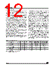
12 / 51 page  M58LW032D 12/51 BUS OPERATIONS There are five standard bus operations that control the memory. Each of these is described in this section, see Tables 3, Bus Operations, for a sum- mary. On Power-up or after a Hardware Reset the mem- ory defaults to Read Array mode (Page Read). Typically glitches of less than 5ns on Chip Enable or Write Enable are ignored by the memory and do not affect bus operations. Bus Read. Bus Read operations are used to out- put the contents of the Memory Array, the Elec- tronic Signature, the Status Register, the Common Flash Interface and the Block Protection Status. A valid bus operation involves setting the desired address on the Address inputs, enabling the de- vice (refer to Table 2, Device Enable), applying a Low signal, VIL, to Output Enable and keeping Write Enable High, VIH. The data read depends on the previous command written to the memory (see Command Interface section). See Figure 9, Bus Read AC Waveforms, and Ta- ble 15, Bus Read AC Characteristics, for details of when the output becomes valid. Bus Write. Bus Write operations write Com- mands to the memory or latch addresses and input data to be programmed. A valid Bus Write operation begins by setting the desired address on the Address Inputs and en- abling the device (refer to Chip Enable section). The Address Inputs are latched by the Command Interface on the rising edge of Write Enable or the first edge of E0, E1 or E2 that disables the device (refer to Table 2, Device Enable). The Data Input/Outputs are latched by the Com- mand Interface on the rising edge of Write Enable or the first edge of E0, E1 or E2 that disables the device whichever occurs first. Output Enable must remain High, VIH, during the Bus Write operation. See Figures 11, and 12, Write AC Waveforms, and Tables 17 and 18, Write and Chip Enable Con- trolled Write AC Characteristics, for details of the timing requirements. Output Disable. The Data Inputs/Outputs are high impedance when the Output Enable is at VIH. Power-Down. The memory is in Power-Down mode when Reset/Power-Down, RP, is Low. The power consumption is reduced to the Power-Down level, IDD2, and the outputs are high impedance, independent of Chip Enable, Output Enable or Write Enable. Standby. Standby disables most of the internal circuitry, allowing a substantial reduction of the current consumption. The memory is in standby when Chip Enable is at VIH. The power consump- tion is reduced to the standby level IDD1 and the outputs are set to high impedance, independently of the Output Enable or Write Enable inputs. If Chip Enable switches to VIH during a program or erase operation, the device enters Standby mode when finished. Table 3. Bus Operations Note: 1. DQ8-DQ15 are High Z in x8 mode. 2. X = Don’t Care VIL or VIH. Bus Operation E0, E1 or E2 G W RP A1-A21 (x16) A0-A21 (x8) DQ0-DQ15 (x16) DQ0-DQ7 (x8)(1) Bus Read VIL VIL VIH VIH Address Data Output Bus Write VIL VIH VIL VIH Address Data Input Output Disable VIL VIH VIH VIH X High Z Power-Down X X X VIL X High Z Standby VIH XX VIH X High Z |
|
Link URL |
| Cho đến nay ALLDATASHEET có giúp ích cho doanh nghiệp của bạn hay không? [ DONATE ] |
Alldatasheet là | Quảng cáo | Liên lạc với chúng tôi | Chính sách bảo mật | Liên kết đến bảng dữ liệu | Trao đổi link | Tìm kiếm theo nhà sản xuất All Rights Reserved©Alldatasheet.com |
| Russian : Alldatasheetru.com | Korean : Alldatasheet.co.kr | Spanish : Alldatasheet.es | French : Alldatasheet.fr | Italian : Alldatasheetit.com Portuguese : Alldatasheetpt.com | Polish : Alldatasheet.pl | Vietnamese : Alldatasheet.vn Indian : Alldatasheet.in | Mexican : Alldatasheet.com.mx | British : Alldatasheet.co.uk | New Zealand : Alldatasheet.co.nz |
|
Family Site : ic2ic.com |
icmetro.com |
 Vietnamese ▼
 English
 Chinese
 German
 Japanese
 Russian
 Korean
 Spanish
 French
 Italian
 Portuguese
 Polish
 Vietnamese
 Indian
 Mexican
 British
 New Zealand