|
công cụ tìm kiếm bảng dữ liệu linh kiện điện tử |
|
|
công cụ tìm kiếm bảng dữ liệu linh kiện điện tử |
|
R3111Q552B bảng dữ liệu(PDF) 42 Page - Nisshinbo Micro Devices Inc. |
|
|
|||||||||||||||||||||||||||||
R3111Q552B bảng dữ liệu(HTML) 42 Page - Nisshinbo Micro Devices Inc. |
|
|
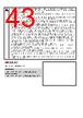
42 / 43 page  R3111x 42 R3111E (TO-92) is the discontinued product as of April, 2017. TECHNICAL NOTES When connecting resistors to the device’s input pin When connecting a resistor (R1) to an input of this device, the input voltage decreases by [Device’s Consumption Current] x [Resistance Value] only. And, the cross conduction current*1, which occurs when changing from the detecting state to the release state, is decreased the input voltage by [Cross Conduction Current] x [Resistance Value] only. And then, this device will enter the re-detecting state if the input voltage reduction is larger than the difference between the detector voltage and the released voltage. When the input resistance value is large and the VDD is gone up at mildly in the vicinity of the released voltage, repeating the above operation may result in the occurrence of output. As shown in Figure A/B, set R1 to become 100 kΩ or less as a guide, and connect CIN of 0.1 μF and more to between the input pin and GND. Besides, make evaluations including temperature properties under the actual usage condition, with using the evaluation board like this way. As a result, make sure that the cross conduction current has no problem. VDD R1 GND OUT pin CIN*2 Figure A Voltage Detector VDD R1 GND OUT pin CIN*2 Figure B Voltage Detector R2 *1 In the CMOS output type, a charging current for OUT pin is included. *2 Note the bias dependence of capacitors. |
|
Link URL |
| Cho đến nay ALLDATASHEET có giúp ích cho doanh nghiệp của bạn hay không? [ DONATE ] |
Alldatasheet là | Quảng cáo | Liên lạc với chúng tôi | Chính sách bảo mật | Liên kết đến bảng dữ liệu | Trao đổi link | Tìm kiếm theo nhà sản xuất All Rights Reserved©Alldatasheet.com |
| Russian : Alldatasheetru.com | Korean : Alldatasheet.co.kr | Spanish : Alldatasheet.es | French : Alldatasheet.fr | Italian : Alldatasheetit.com Portuguese : Alldatasheetpt.com | Polish : Alldatasheet.pl | Vietnamese : Alldatasheet.vn Indian : Alldatasheet.in | Mexican : Alldatasheet.com.mx | British : Alldatasheet.co.uk | New Zealand : Alldatasheet.co.nz |
|
Family Site : ic2ic.com |
icmetro.com |
 Vietnamese ▼
 English
 Chinese
 German
 Japanese
 Russian
 Korean
 Spanish
 French
 Italian
 Portuguese
 Polish
 Vietnamese
 Indian
 Mexican
 British
 New Zealand