|
công cụ tìm kiếm bảng dữ liệu linh kiện điện tử |
|
|
công cụ tìm kiếm bảng dữ liệu linh kiện điện tử |
|
IS25LE512M-RLLA3:P-TY bảng dữ liệu(PDF) 145 Page - Integrated Silicon Solution, Inc |
|
|
|||||||||||||||||||||||||||||
IS25LE512M-RLLA3:P-TY bảng dữ liệu(HTML) 145 Page - Integrated Silicon Solution, Inc |
|
|
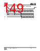
145 / 189 page  IS25LE512M IS25WE512M Integrated Silicon Solution, Inc.- www.issi.com 145 Rev. A6 06/16/2025 8.47 WRITE BANK ADDRESS REGISTER OPERATION (WRBRNV: 18h, WRBRV: 17h/C5h) The Write Bank Address Register (WRBRNV and WRBRV) instruction is used to write address bits above A23, into the Bank Address Register (BAR). WRBRNV is used to write the non-volatile Bank Address Register and WRBRV is used to write the volatile Bank Address Register. The instruction is also used to write the Extended Address Control bit (EXTADD) that is also in BAR [7]. BAR provides the high order addresses needed by devices having more than 128Mbits (16Mbytes), when using 3-byte address commands without extended addressing enabled (BAR [7] EXTADD = 0). To write non-volatile Bank Address Register, a standard Write Enable (06h) instruction must previously have been executed for the device to accept WRBRNV(18h) instruction (Status Register bit WEL must equal “1”). To write volatile Bank Address Register, C5h or 17h command can be used. When using C5h instruction, a standard Write Enable (06h) instruction must previously have been executed for the device to accept C5h instruction (Status Register bit WEL mus t equal “1”). But 17h instruction does not require a standard Write Enable (06h) operation. (Status Register bit WEL remains “0”). The WRBRNV/WRBRV instructions are followed by the data byte. The Bank Address Register is one data byte in length. The Write In Progress (WIP) bit is “1” during WRBRNV/WRBRV operation, and is “0” when it is completed. Any bank address bit reserved for the future should always be written as “0”. Data is shifted in from SI and in SPI whereas data is shifted in via four pins (IO0-IO3) in QPI. Bit 7 (EXTADD) of volatile Bank Address Register is also writable with EN4B (B7h)/EX4B (29h) instruction. But B7h/29h instruction does not require a standard Write Enable (06h) (Status Register bit WEL remains 0). Note: When WRBRNV is executed, the volatile Bank Address Register is set as well as the non-volatile Bank Address Register. Figure 8.104 Write Bank Address Register Sequence In SPI Mode Instruction = 18h or 17h/C5h CE # SCK SI SO Data In 0 1 2 3 4 5 6 7 8 9 10 11 12 13 14 15 Mode 3 Mode 0 7 3 2 1 0 6 5 4 High Impedence Figure 8.105 Write Bank Address Register Sequence In QPI Mode 18h or 17h/C5h 0 1 Mode 3 Mode 0 2 3 7:4 3:0 CE# SCK IO[3:0] Data In |
|
Link URL |
| Cho đến nay ALLDATASHEET có giúp ích cho doanh nghiệp của bạn hay không? [ DONATE ] |
Alldatasheet là | Quảng cáo | Liên lạc với chúng tôi | Chính sách bảo mật | Liên kết đến bảng dữ liệu | Trao đổi link | Tìm kiếm theo nhà sản xuất All Rights Reserved©Alldatasheet.com |
| Russian : Alldatasheetru.com | Korean : Alldatasheet.co.kr | Spanish : Alldatasheet.es | French : Alldatasheet.fr | Italian : Alldatasheetit.com Portuguese : Alldatasheetpt.com | Polish : Alldatasheet.pl | Vietnamese : Alldatasheet.vn Indian : Alldatasheet.in | Mexican : Alldatasheet.com.mx | British : Alldatasheet.co.uk | New Zealand : Alldatasheet.co.nz |
|
Family Site : ic2ic.com |
icmetro.com |
 Vietnamese ▼
 English
 Chinese
 German
 Japanese
 Russian
 Korean
 Spanish
 French
 Italian
 Portuguese
 Polish
 Vietnamese
 Indian
 Mexican
 British
 New Zealand