|
công cụ tìm kiếm bảng dữ liệu linh kiện điện tử |
|
|
công cụ tìm kiếm bảng dữ liệu linh kiện điện tử |
|
ADBMS1818ASWZ-R7 bảng dữ liệu(PDF) 7 Page - Analog Devices |
|
|
|||||||||||||||||||||||||||||
ADBMS1818ASWZ-R7 bảng dữ liệu(HTML) 7 Page - Analog Devices |
|
|
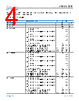
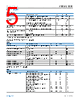
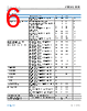
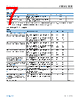
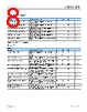
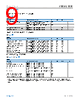
7 / 92 page  Data Sheet ADBMS1818 SPECIFICATIONS analog.com Rev. B | 7 of 92 Table 3. (Continued) Parameter Test Conditions/Comments Min Typ Max Unit Watchdog Timer Pin Low (VOL(WDT)) WDT pin sinking 4 mA, apply over the full specified temperature range 0.4 V General-Purpose I/O Pin Low (VOL(GPIO)) GPIO pin sinking 4 mA (used as digital output), apply over the full specified temperature range 0.4 V 1 The active state current is calculated from dc measurements. The active state current is the additional average supply current into VREG when there are continuous 1 MHz communications on the isoSPI ports with 50% data 1s and 50% data 0s. Slower clock rates reduce the supply current. ADC TIMING SPECIFICATIONS Table 4. Parameter Test Conditions/Comments Min Typ Max Unit (tCYCLE) (See Figure 55, Figure 56, and Figure 58) Measurement and Calibration Cycle Time When Starting from the REFUP State in Normal Mode Measure 18 cells, apply over the full specified temperature range 2027 2343 2488 µs Measure 3 cells, apply over the full specified temperature range 352 407 432 µs Measure 18 cells and 2 GPIO inputs, apply over the full specified temperature range 2717 3140 3335 µs Measurement and Calibration Cycle Time When Starting from the REFUP State in Filtered Mode Measure 18 cells, apply over the full specified temperature range 174.2 201.3 213.8 ms Measure 3 cells, apply over the full specified temperature range 29.1 33.6 35.7 ms Measure 18 cells and 2 GPIO inputs, apply over the full specified temperature range 232.3 268.5 285.1 ms Measurement and Calibration Cycle Time When Starting from the REFUP State in Fast Mode Measure 18 cells, apply over the full specified temperature range 970 1121 1191 µs Measure 3 cells, apply over the full specified temperature range 176 203 215 µs Measure 18 cells and 2 GPIO inputs, apply over the full specified temperature range 1307 1511 1605 µs Skew Time (tSKEW1). The Time Difference Between Cell 18 and GPIO1 Measurements, Command = ADCVAX (See Figure 58) Fast mode, apply over the full specified temperature range 168 194 206 µs Normal mode, apply over the full specified temperature range 470 543 577 µs Skew Time(tSKEW2). The Time Difference Between Cell 18 and Cell 1 Measurements, Command = ADCV (See Figure 55) Fast mode, apply over the full specified temperature range 202 233 248 µs Normal mode, apply over the full specified temperature range 580 670 711 µs Regulator Start-Up Time (tWAKE) VREG generated from the DRIVE pin (see Figure 93), apply over the full specified temperature range 200 400 µs Watchdog or Discharge Timer (tSLEEP) (See Figure 87) DTEN pin = 0 or DCTO, Bits[3:0] = 0000, apply over the full specified temperature range 1.8 2 2.2 sec DTEN pin = 1 and DCTO, Bits[3:0] ≠ 0000 0.5 120 min Reference Wake-Up Time (tREFUP (See Figure 55)). Added to tCYCLE Time When Starting from the Standby State. tREFUP = 0 When Starting from Other States tREFUP is independent of the number of channels measured and the ADC mode, apply over the full specified temperature range 2.7 3.5 4.4 ms ADC Clock Frequency (fS) 3.3 MHz |
|
Link URL |
| Cho đến nay ALLDATASHEET có giúp ích cho doanh nghiệp của bạn hay không? [ DONATE ] |
Alldatasheet là | Quảng cáo | Liên lạc với chúng tôi | Chính sách bảo mật | Liên kết đến bảng dữ liệu | Trao đổi link | Tìm kiếm theo nhà sản xuất All Rights Reserved©Alldatasheet.com |
| Russian : Alldatasheetru.com | Korean : Alldatasheet.co.kr | Spanish : Alldatasheet.es | French : Alldatasheet.fr | Italian : Alldatasheetit.com Portuguese : Alldatasheetpt.com | Polish : Alldatasheet.pl | Vietnamese : Alldatasheet.vn Indian : Alldatasheet.in | Mexican : Alldatasheet.com.mx | British : Alldatasheet.co.uk | New Zealand : Alldatasheet.co.nz |
|
Family Site : ic2ic.com |
icmetro.com |
 Vietnamese ▼
 English
 Chinese
 German
 Japanese
 Russian
 Korean
 Spanish
 French
 Italian
 Portuguese
 Polish
 Vietnamese
 Indian
 Mexican
 British
 New Zealand