|
công cụ tìm kiếm bảng dữ liệu linh kiện điện tử |
|
|
công cụ tìm kiếm bảng dữ liệu linh kiện điện tử |
|
ADRF6720ACPZ-R7 bảng dữ liệu(PDF) 9 Page - Analog Devices |
|
|
|||||||||||||||||||||||||||||
ADRF6720ACPZ-R7 bảng dữ liệu(HTML) 9 Page - Analog Devices |
|
|
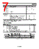
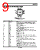
9 / 44 page  Data Sheet ADRF6720 PIN CONFIGURATION AND FUNCTION DESCRIPTIONS Figure 3. Pin Configuration Table 5. Pin Function Descriptions Pin No. Mnemonic Description 1 MUXOUT Multiplexer Output. This output allows a digital lock detect signal, a voltage proportional to absolute temperature (VPTAT), or a buffered, frequency-scaled reference signal to be accessed externally. The output is selected by programming Bits[6:4] in Register 0x21. 2, 10 GND Baseband Ground. 3, 4 I+, I− Differential In-Phase Baseband Inputs. 5, 7 GND Mixer Core (I and Q) Ground. 6 VPOS1 3.3 V Supply Voltage for Baseband. Decouple VPOS1 with 100 pF and 0.1 µF capacitors located close to the pin. 8, 9 Q−, Q+ Differential Quadrature Baseband Inputs. 11 VPOS2 3.3 V Supply Voltage for 2.5 V LDO. Decouple VPOS2 with 100 pF and 0.1 µF capacitors located close to the pin. 12 DECL1 Decoupling Pin for 2.5 V LDO. Connect 100 pF, 0.1 µF, and 10 µF capacitors between this pin and ground. 13 SDIO Serial Data Input/Output for SPI. 14 SCLK Serial Clock Input/Output for SPI. 15 CS Chip Select Input/Output for SPI. 16 GND Digital Ground. 17 VPOS3 3.3 V Supply Voltage for LO. Decouple VPOS3 with 100 pF and 0.1 µF capacitors located close to the pin. 18, 19 LOOUT+, LOOUT− Differential LO Outputs. Either the internally generated LO or external 1 × LO/2 × LO is available at 1 × LO or 2 × LO on these pins. 20 GND LO Ground. 21 NIC Not Internally Connected. This pin can be left open or tied to RF ground. 22 VPOS4 3.3 V Supply Voltage for RF. Decouple VPOS4 with 100 pF and 0.1 µF capacitors located close to the pin. 23, 25 GND RF Ground. 24 RFOUT Single-Ended 0 V DC RF Output. 26 VPOS5 3.3 V Supply Voltage for RF. Decouple VPOS5 with 100 pF and 0.1 µF capacitors located close to the pin. 27 ENBL Enables/Disables the Circuit Blocks. References the settings at Register 0x01 and Register 0x10. Refer to the ENBL section for more information. 28 DECL2 Decoupling Pin for VCO LDO. Connect 100 pF, 0.1 µF, and 10 µF capacitors between this pin and ground. 29 GND VCO Ground. 1. NIC = NOT INTERNALLY CONNECTED. MUXOUT GND I+ I– GND VPOS1 GND Q+ Q– GND GND RFOUT GND VPOS5 NIC DECL2 GND VPOS6 VPOS4 ENBL NOTES 2. SOLDER THE EXPOSED PAD TO A LOW IMPEDANCE GROUND PLANE. 1 2 3 4 5 6 7 8 9 10 23 24 25 26 27 28 29 30 22 21 ADRF6720 TOP VIEW (Not to Scale) Rev. 0 | Page 9 of 44 |
|
Link URL |
| Cho đến nay ALLDATASHEET có giúp ích cho doanh nghiệp của bạn hay không? [ DONATE ] |
Alldatasheet là | Quảng cáo | Liên lạc với chúng tôi | Chính sách bảo mật | Liên kết đến bảng dữ liệu | Trao đổi link | Tìm kiếm theo nhà sản xuất All Rights Reserved©Alldatasheet.com |
| Russian : Alldatasheetru.com | Korean : Alldatasheet.co.kr | Spanish : Alldatasheet.es | French : Alldatasheet.fr | Italian : Alldatasheetit.com Portuguese : Alldatasheetpt.com | Polish : Alldatasheet.pl | Vietnamese : Alldatasheet.vn Indian : Alldatasheet.in | Mexican : Alldatasheet.com.mx | British : Alldatasheet.co.uk | New Zealand : Alldatasheet.co.nz |
|
Family Site : ic2ic.com |
icmetro.com |
 Vietnamese ▼
 English
 Chinese
 German
 Japanese
 Russian
 Korean
 Spanish
 French
 Italian
 Portuguese
 Polish
 Vietnamese
 Indian
 Mexican
 British
 New Zealand