|
công cụ tìm kiếm bảng dữ liệu linh kiện điện tử |
|
|
công cụ tìm kiếm bảng dữ liệu linh kiện điện tử |
|
ADRF6720ACPZ-R7 bảng dữ liệu(PDF) 24 Page - Analog Devices |
|
|
|||||||||||||||||||||||||||||
ADRF6720ACPZ-R7 bảng dữ liệu(HTML) 24 Page - Analog Devices |
|
|
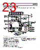
24 / 44 page  ADRF6720 Data Sheet BASEBAND INPUTS Drive the four I and Q inputs with an external bias level of 500 mV. These inputs are generally dc-coupled to the outputs of a dual DAC. The nominal drive level used in the characterization of the ADRF6720 is 1 V p-p differential (or 500 mV p-p on each pin). The I and Q input resistances are 500 Ω, differential. As a result, the external shunt resistors at the I and Q inputs may be required to interface a DAC or a filter. The effective value of the resistance is 500 Ω in parallel with the shunt resistor (see the DAC to I/Q Modulator Interfacing section for more information). LO INPUT The external LO input is designed to be driven differentially. AC couple both sides of the differential LO source through a pair of series capacitors to the LOIN+ and LOIN− pins. The typical LO drive level, used for the characterization of the ADRF6720, is 0 dBm. Apply the reference frequency for the PLL (between 5.7 MHz and 320 MHz) to the REFIN pin, which is ac-coupled. If the REFIN pin is being driven from a 50 Ω source, terminate the pin with 50 Ω as shown in Figure 44. Apply a drive level of about 4 dBm to 14 dBm; 4 dBm is used at characterization. LOOP FILTER The loop filter in Figure 44 is connected between the CP and VTUNE pins. The recommended components for 20 kHz filter designs are shown in Table 8. RF OUTPUT The RF output is available at the RFOUT pin (Pin 24), which can drive a 50 Ω load. Rev. 0 | Page 24 of 44 |
|
Link URL |
| Cho đến nay ALLDATASHEET có giúp ích cho doanh nghiệp của bạn hay không? [ DONATE ] |
Alldatasheet là | Quảng cáo | Liên lạc với chúng tôi | Chính sách bảo mật | Liên kết đến bảng dữ liệu | Trao đổi link | Tìm kiếm theo nhà sản xuất All Rights Reserved©Alldatasheet.com |
| Russian : Alldatasheetru.com | Korean : Alldatasheet.co.kr | Spanish : Alldatasheet.es | French : Alldatasheet.fr | Italian : Alldatasheetit.com Portuguese : Alldatasheetpt.com | Polish : Alldatasheet.pl | Vietnamese : Alldatasheet.vn Indian : Alldatasheet.in | Mexican : Alldatasheet.com.mx | British : Alldatasheet.co.uk | New Zealand : Alldatasheet.co.nz |
|
Family Site : ic2ic.com |
icmetro.com |
 Vietnamese ▼
 English
 Chinese
 German
 Japanese
 Russian
 Korean
 Spanish
 French
 Italian
 Portuguese
 Polish
 Vietnamese
 Indian
 Mexican
 British
 New Zealand