|
công cụ tìm kiếm bảng dữ liệu linh kiện điện tử |
|
|
công cụ tìm kiếm bảng dữ liệu linh kiện điện tử |
|
AD9577BCPZ-R7 bảng dữ liệu(PDF) 41 Page - Analog Devices |
|
|
|||||||||||||||||||||||||||||
AD9577BCPZ-R7 bảng dữ liệu(HTML) 41 Page - Analog Devices |
|
|
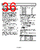
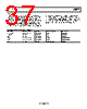
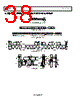
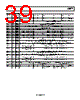
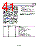
41 / 44 page  Data Sheet AD9577 Rev. 0 | Page 41 of 44 The AD9577 acts as a standard slave device on the bus. The data on the SDA pin is eight bits long supporting the 7-bit addresses plus the R/W bit. The has 31 subaddresses to enable the user-accessible internal registers (see ). Therefore, it interprets the first byte as the device address and the second byte as the starting subaddress. Auto-increment mode is supported, which allows data to be read from or written to the starting subaddress and each subsequent address without manually addressing the subsequent subaddress. A data transfer is always terminated by a stop condition. The user can also access any unique subaddress register on a one-by-one basis without updating all registers. AD9577 Table 30 Stop and start conditions can be detected at any stage of the data transfer. If these conditions are asserted out of sequence with normal read and write operations, they cause an immediate jump to the idle condition. During a given SCL high period, one start condition, one stop condition, or a single stop condition followed by a single start condition should be issued. If an invalid subaddress is issued, the AD9577 does not issue an acknowledge and returns to the idle condition. If the highest subaddress is exceeded while reading back in auto-increment mode, the highest subaddress register contents continue to be output until the master device issues a no acknowledge, which indicates the end of a read. In a no acknowledge condition, the SDA line is not pulled low on the ninth pulse. See Figure 45 and Figure 46 for sample read and write data transfers, and see Figure 47 for a more detailed timing diagram. To overwrite any of the default register values, complete the following steps: 1. Enable the overwriting of registers by setting EnI2C, Register C0[1]. 2. Only write to registers that need modification from their default value. 3. After all the registers have been set, a new acquisition is initiated by toggling NewAcq, Register X0[0] from low to high to low. An example set of I2C commands follows. These enable the I2C registers and program the output frequencies of both PLLs. fPFD is 25 MHz. A leading W represents a write command. Table 32. I2C Programming Example Register Writes Write/Read Register Name Data (Hex) Operation W C0 02 Enable I2C registers W AF0 0A Na = 80 + 10 = 90; fVCO1 = 2.25 GHz W ADV0 A6 Channel 0 divides by 5 × 6 = 30; fOUT0 = 75 MHz W ADV1 CC Channel 1 divides by 6 × 12 = 72; fOUT1 = 31.25 MHz W BF3 15 Nb = 80 + 21 = 101; FVCO2 = 2.53832 GHz W BF0 14 FRAC = 333 W BF1 D2 FRAC = 333, MOD = 625 W BF2 71 MOD = 625 W ABF0 C0 Power-up SDM, release SDM reset W BP0 04 Turn on Bleed W BDV0 44 Channel 2 divides by 2 × 4 = 8; fOUT2 = 317.29 MHz W BDV1 B0 Channel 3 divides by 5 × 16 = 80; fOUT3 = 31.729 MHz W X0 01 Force new acquisition by toggling NewAcq W X0 00 |
|
Link URL |
| Cho đến nay ALLDATASHEET có giúp ích cho doanh nghiệp của bạn hay không? [ DONATE ] |
Alldatasheet là | Quảng cáo | Liên lạc với chúng tôi | Chính sách bảo mật | Liên kết đến bảng dữ liệu | Trao đổi link | Tìm kiếm theo nhà sản xuất All Rights Reserved©Alldatasheet.com |
| Russian : Alldatasheetru.com | Korean : Alldatasheet.co.kr | Spanish : Alldatasheet.es | French : Alldatasheet.fr | Italian : Alldatasheetit.com Portuguese : Alldatasheetpt.com | Polish : Alldatasheet.pl | Vietnamese : Alldatasheet.vn Indian : Alldatasheet.in | Mexican : Alldatasheet.com.mx | British : Alldatasheet.co.uk | New Zealand : Alldatasheet.co.nz |
|
Family Site : ic2ic.com |
icmetro.com |
 Vietnamese ▼
 English
 Chinese
 German
 Japanese
 Russian
 Korean
 Spanish
 French
 Italian
 Portuguese
 Polish
 Vietnamese
 Indian
 Mexican
 British
 New Zealand