|
công cụ tìm kiếm bảng dữ liệu linh kiện điện tử |
|
|
công cụ tìm kiếm bảng dữ liệu linh kiện điện tử |
|
ACS8946 bảng dữ liệu(PDF) 9 Page - Semtech Corporation |
|
|
|||||||||||||||||||||||||||||
ACS8946 bảng dữ liệu(HTML) 9 Page - Semtech Corporation |
|
|
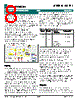
9 / 40 page  ADVANCED COMMUNICATIONS FINAL DATASHEET Revision 3/November 2006 © Semtech Corp. Page 9 www.semtech.com ACS8946 JAM PLL also possible using suitable passive components (see “Input and Output Interface Terminations” on page 27). Output clock rates at 19.44 MHz, 38.88 MHz, 77.76 MHz, 125.00 MHz, 155.52 MHz, 156.25 MHz, 311.04 MHz, 622.08 MHz or 625.00 MHz are selectable. Additionally, odd number division of these frequencies up to divide-by- 15 can also be configured. Note that if odd number division is used, the frequency adjustment factor will apply to all outputs, adjusting all selected output frequencies proportionally. The output frequency of each output is determined by a combination of the wiring of the configuration pins CFG_IN[7:0] read at power-up, and state of the asynchronously set RATE[2:1]A and RATE[2:1]B pins. The user configures a set of “Available Rates” (four frequencies that are available for selection at every Clock Output) and then configures each output individually to output one of these four rates. OUT1 and OUT2 are asynchronously controllable allowing the output frequency to be switched among the “Available Rates” under control from the rate selection pins (RATE[2:1]A and RATE[2:1]B). To determine the correct wiring of configuration pins to configure the device involves the use of several look-up tables, and for completeness the datasheet includes all of these, with worked examples (See “Configuration” on page 13). However, to make configuring the device much more simple than this description and look-up tables suggest, Semtech provides a user-friendly Graphical User Interface (GUI) software package to accompany the ACS8946 in which the User enters the required I/O frequencies, dividers settings etc. as required for a particular application, and the GUI responds by displaying the interconnections required to achieve that configuration. Refer to the ACS8946 EVB Document and associated software. Unused outputs should be left floating with their associated VDD connected to GND. For example, if OUT4 is not required, connect VDD04 to GND and leave OUT4N and OUT4P unconnected. Clock Multiplication The ACS8946 provides options to multiply a 19.44 MHz input by 2, 4, 8, 16, or 32 for standard SONET SDH spot frequency configurations. 125.00 MHz dejittered output for Gigabit Ethernet (GbE/10 GbE) is also supported if 125.00 MHz is provided as the input reference, and 156.25 MHz input (for 12.5 GbE) is also supported. These rates are configured by the wiring of CFG_IN[3:2], see Table 10. If the input frequency used is a percentage away from the configured spot frequency, then the resulting output frequency will change by the same percentage. Refer back to Table 5 for permitted input frequencies. Note...GbE rates are not directly available as conversions from SONET/SDH rates. Voltage Controlled Oscillator The internal VCO operates at 2.48832 GHz when the device is configured for standard SONET/SDH spot frequencies. The VCO frequency is divided down to the selected rate giving a precise 50/50 balanced mark/space ratio for the output. For 125.00 MHz operation the VCO operates at 2.500 GHz. Jitter Filtering Input jitter is attenuated by the PLL with the frequency cut- off point (Fc), at which jitter is either tracked or attenuated, defined by the -3 dB point i.e. the position of the first pole of the PLL loop filter. The bandwidth (frequency at which the first pole occurs) is defined by the component value selected for the filter in Tables 6 and 7. For 19.44 MHz input, using a loop filter bandwidth of 2 kHz and damping factor of 1.2 gives: High input jitter attenuation and roll off: • - 20 dB/decade from first loop filter pole, (Fc) • - 40 dB/decade from 2nd pole (typically 10 x Fc) Jitter peaking is less than 1 dB (dependent on the loop filter components) Table 5 Permitted Input Frequency Range Selected Input Spot Frequency/ MHz Selected FEC Ratio (*or Divider Ratio using Odd Divider) Max and Min Permitted Input Frequency Expressed as a Percentage Above (+%) or Below (-%) the Selected Input Spot Frequency +% -% 19.44, 38.88 77.76, 155.52 1:1 12.0 3.0 125.00 5:4* 10.0 3.0 156.25 1:1 12.0 3.0 |
|
Link URL |
| Cho đến nay ALLDATASHEET có giúp ích cho doanh nghiệp của bạn hay không? [ DONATE ] |
Alldatasheet là | Quảng cáo | Liên lạc với chúng tôi | Chính sách bảo mật | Liên kết đến bảng dữ liệu | Trao đổi link | Tìm kiếm theo nhà sản xuất All Rights Reserved©Alldatasheet.com |
| Russian : Alldatasheetru.com | Korean : Alldatasheet.co.kr | Spanish : Alldatasheet.es | French : Alldatasheet.fr | Italian : Alldatasheetit.com Portuguese : Alldatasheetpt.com | Polish : Alldatasheet.pl | Vietnamese : Alldatasheet.vn Indian : Alldatasheet.in | Mexican : Alldatasheet.com.mx | British : Alldatasheet.co.uk | New Zealand : Alldatasheet.co.nz |
|
Family Site : ic2ic.com |
icmetro.com |
 Vietnamese ▼
 English
 Chinese
 German
 Japanese
 Russian
 Korean
 Spanish
 French
 Italian
 Portuguese
 Polish
 Vietnamese
 Indian
 Mexican
 British
 New Zealand