|
công cụ tìm kiếm bảng dữ liệu linh kiện điện tử |
|
|
công cụ tìm kiếm bảng dữ liệu linh kiện điện tử |
|
PI2EQX5864 bảng dữ liệu(PDF) 9 Page - Pericom Semiconductor Corporation |
|
|
|||||||||||||||||||||||||||||
PI2EQX5864 bảng dữ liệu(HTML) 9 Page - Pericom Semiconductor Corporation |
|
|
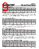
9 / 18 page  9 PS8934A 01/21/08 PI2EQX5864 5.0Gbps 4-Lane PCI Express GenII Re-Driver with Equalization, Emphasis and I2C Control BYTE 6 - Power Down Control (PWR) PD_xy# =0=channel off/power down, PD_xy# =1=normal operation, Latch from PD# input at startup Bit 7 6 5 4 3 2 1 0 Name PD_A0# PD_B0# PD_A1# PD_B1# PD_A2# PD_B2# PD_A3# PD_B3# Type R/W R/W R/W R/W R/W R/W R/W R/W Power-on State 111 1 1 1 1 1 Note: R=Read only, W=Write only, R/W=Read and Write, X=Undefined, rsvd=reserved for future use The Power Down Control register allows for individual control over each channel for power savings. When PD_xy# is logic 0 the channel is turned off. When PD_xy# is 1 then the channel is enabled for normal operation. BYTE 7 - Receiver Detect Enable (RXD) RXD_xy =0=channel off/power down, RXD_xy =1=normal operation, Latch from PD# input at startup Bit 7 6 5 4 3 2 1 0 Name RXD_A0 RXD_B0 RXD_A1 RXD_B1 RXD_A2 RXD_B2 RXD_A3 RXD_B3 Type R/W R/W R/W R/W R/W R/W R/W R/W Power-on State 11 1 1 1 1 1 1 Note: R=Read only, W=Write only, R/W=Read and Write, X=Undefined, rsvd=reserved for future use The Receiver Detect Enable register allows for control of the receiver detect state machine for each individual channel. When RXD_xy is set to 0, then the receiver detect function is disabled. When RXD_xy is logic 1, then the receiver detect state machine is enabled for operation. The initial state of the register bits are determined by the RXD_A and RXD_B input pins during power-up. BYTE 8 - A-Channels Equalizer and Output Control (AEOC) SELx_A: Equalizer configuration, Dx_A: Emphasis control, Sx_A: Output level control (see Configuration Table) Bit 7 6 5 4 3 2 1 0 Name SEL0_A SEL1_A SEL2_A D0_A D1_A D2_A S0_A S1_A Type R/W R/W R/W R/W R/W R/W R/W R/W Power-on State 11 1 1 1 1 1 1 Note: R=Read only, W=Write only, R/W=Read and Write, X=Undefined, rsvd=reserved for future use BYTE 5 - Channel Reset (RESET) RES_xy# =0=reset, RES_xy# =1=normal operation. Latch from RES_A# & RES_B# inputs at startup Bit 7 6 5 4 3 2 1 0 Name RES_A0# RES_B0# RES_A1# RES_B1# RES_A2# RES_B2# RES_A3# RES_B3# Type R/W R/W R/W R/W R/W R/W R/W R/W Power-on State 111 1 1 1 1 1 Note: R=Read only, W=Write only, R/W=Read and Write, X=Undefined, rsvd=reserved for future use The Channel Reset register allows for restart of an individual channels Receiver Detect function. A transition from 0 to 1 initiates a new Receiver Detect cycle (if the channel is enabled and receiver detect is enabled). While static at 0 or 1, the RES_zy# bit will have no effect on operation. The Channel Reset bits are read/write allowing the current state to be checked. 07-0277 |
|
|
Link URL |
| Cho đến nay ALLDATASHEET có giúp ích cho doanh nghiệp của bạn hay không? [ DONATE ] |
Alldatasheet là | Quảng cáo | Liên lạc với chúng tôi | Chính sách bảo mật | Liên kết đến bảng dữ liệu | Trao đổi link | Tìm kiếm theo nhà sản xuất All Rights Reserved©Alldatasheet.com |
| Russian : Alldatasheetru.com | Korean : Alldatasheet.co.kr | Spanish : Alldatasheet.es | French : Alldatasheet.fr | Italian : Alldatasheetit.com Portuguese : Alldatasheetpt.com | Polish : Alldatasheet.pl | Vietnamese : Alldatasheet.vn Indian : Alldatasheet.in | Mexican : Alldatasheet.com.mx | British : Alldatasheet.co.uk | New Zealand : Alldatasheet.co.nz |
|
Family Site : ic2ic.com |
icmetro.com |
 Vietnamese ▼
 English
 Chinese
 German
 Japanese
 Russian
 Korean
 Spanish
 French
 Italian
 Portuguese
 Polish
 Vietnamese
 Indian
 Mexican
 British
 New Zealand