|
công cụ tìm kiếm bảng dữ liệu linh kiện điện tử |
|
|
công cụ tìm kiếm bảng dữ liệu linh kiện điện tử |
|
SAA3010 bảng dữ liệu(PDF) 6 Page - NXP Semiconductors |
|
|
|||||||||||||||||||||||||||||
SAA3010 bảng dữ liệu(HTML) 6 Page - NXP Semiconductors |
|
|
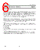
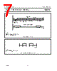
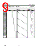
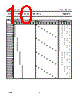
6 / 20 page  June 1989 6 Philips Semiconductors Product specification Infrared remote control transmitter RC-5 SAA3010 FUNCTIONAL DESCRIPTION Keyboard operation Every connection of one X-input and one DR-output will be recognized as a legal key operation and will cause the device to generate the corresponding code. The same applies to every connection of one Z-input to one DR-output with the proviso that SSM must be LOW. When SSM is HIGH a wired connection must exist between a Z-input and a DR-output. If no connection is present the system number will not be generated. Activating two or more X-inputs, Z-inputs or Z-inputs and X-inputs at the same time is an illegal action and inhibits further activity (oscillator will not start). When one X- or Z-input is connected to more than one DR-output, the last scan signal will be considered as legal. The maximum value of the contact series resistance of the switched keyboard is 7 k Ω. Inputs In the quiescent state the command inputs X0 to X7 are held HIGH by an internal pull-up transistor. When the system mode selection (SSM) input is LOW and the system is quiescent, the system inputs Z0 to Z3 are also held HIGH by an internal pull-up transistor. When SSM is HIGH the pull-up transistor for the Z-inputs is switched off, in order to prevent current flow, and a wired connection in the Z-DR matrix provides the system number. Outputs The output signal DATA transmits the generated information in accordance with the format illustrated by Fig.4 and Tables 1 and 2. The code is transmitted using a biphase technique as illustrated by Fig.5. The code consists of four parts: • Start part −1.5 bits (2 × logic 1) • Control part −1 bit • System part −5 bits • Command part −6 bits The output signal MDATA transmits the generated information modulated by 1/12 of the oscillator frequency with a 50% duty factor. In the quiescent state both DATA and MDATA are non-conducting (3-state outputs). The scan driver outputs DR0 to DR7 are open drain n-channel transistors and conduct when the circuit is quiescent. After a legal key operation the scanning cycle is started and the outputs switched to the conductive state one by one. The DR-outputs were switched off at the end of the preceding debounce cycle. |
|
|
Link URL |
| Cho đến nay ALLDATASHEET có giúp ích cho doanh nghiệp của bạn hay không? [ DONATE ] |
Alldatasheet là | Quảng cáo | Liên lạc với chúng tôi | Chính sách bảo mật | Liên kết đến bảng dữ liệu | Trao đổi link | Tìm kiếm theo nhà sản xuất All Rights Reserved©Alldatasheet.com |
| Russian : Alldatasheetru.com | Korean : Alldatasheet.co.kr | Spanish : Alldatasheet.es | French : Alldatasheet.fr | Italian : Alldatasheetit.com Portuguese : Alldatasheetpt.com | Polish : Alldatasheet.pl | Vietnamese : Alldatasheet.vn Indian : Alldatasheet.in | Mexican : Alldatasheet.com.mx | British : Alldatasheet.co.uk | New Zealand : Alldatasheet.co.nz |
|
Family Site : ic2ic.com |
icmetro.com |
 Vietnamese ▼
 English
 Chinese
 German
 Japanese
 Russian
 Korean
 Spanish
 French
 Italian
 Portuguese
 Polish
 Vietnamese
 Indian
 Mexican
 British
 New Zealand