|
công cụ tìm kiếm bảng dữ liệu linh kiện điện tử |
|
|
công cụ tìm kiếm bảng dữ liệu linh kiện điện tử |
|
NCV7728DPAR2G bảng dữ liệu(PDF) 17 Page - ON Semiconductor |
|
|
|||||||||||||||||||||||||||||
NCV7728DPAR2G bảng dữ liệu(HTML) 17 Page - ON Semiconductor |
|
|
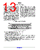
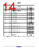
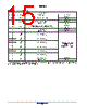
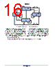
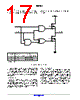
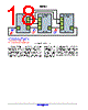
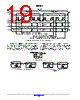
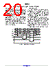
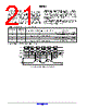
17 / 27 page  NCV7728 www.onsemi.com 17 Driver Control The NCV7728 has the flexibility of controlling each driver through the 16 bit SPI frame (Bits 12−1) and the logic combination required for bridge control is defined in Figure 15. HBENx HBCNFx OUTx VS HSx LSx HBENx HBCNFx OUTx 0 ‘X’ OUTx in High Impedance State 1 0 HSx Off and LSx On 1 1 HSx On and LSx Off ‘X’ = Don’t Care Figure 15. Bridge Control Logic The digital design insures that the high side and low side of the same half bridge will not be active at the same time. Thus the device self protects from a current shoot through condition. Delays (ThsOffLsOn and TlsOffHsOn) between the high side and low side switching are implemented for same reasons. Frame Detection To maintain the data integrity, the NCV7728 has 16 bit frame detection. A valid frame for a single CSB cycle requires 16 bits to be clocked into SI for the initial 16 bits and n x 8 bits thereafter. In an instance of an invalid SPI frame the entire frame is ignored, but the previous states of the corresponding outputs are maintained. Daisy Chain Operation Daisy chain communications between multiple of 8−bit SPI compatible IC’s is possible by connection of the serial output pin (SO) to the input of the sequential IC (SI). The clock phase and clock polarity respect to the data must be the same for all the devices on the chain. Figure 16 illustrates the hardware configuration of NCV7728 daisy chained with a n*8 bit (ie n = 2; 16 bit) SPI device. The progression of data from the MCU through the sequential devices is also shown. Strict adherence to the frame format illustrated in Figure 17 is required for the proper serial daisy chain operations. |
|
Link URL |
| Cho đến nay ALLDATASHEET có giúp ích cho doanh nghiệp của bạn hay không? [ DONATE ] |
Alldatasheet là | Quảng cáo | Liên lạc với chúng tôi | Chính sách bảo mật | Liên kết đến bảng dữ liệu | Trao đổi link | Tìm kiếm theo nhà sản xuất All Rights Reserved©Alldatasheet.com |
| Russian : Alldatasheetru.com | Korean : Alldatasheet.co.kr | Spanish : Alldatasheet.es | French : Alldatasheet.fr | Italian : Alldatasheetit.com Portuguese : Alldatasheetpt.com | Polish : Alldatasheet.pl | Vietnamese : Alldatasheet.vn Indian : Alldatasheet.in | Mexican : Alldatasheet.com.mx | British : Alldatasheet.co.uk | New Zealand : Alldatasheet.co.nz |
|
Family Site : ic2ic.com |
icmetro.com |
 Vietnamese ▼
 English
 Chinese
 German
 Japanese
 Russian
 Korean
 Spanish
 French
 Italian
 Portuguese
 Polish
 Vietnamese
 Indian
 Mexican
 British
 New Zealand