|
công cụ tìm kiếm bảng dữ liệu linh kiện điện tử |
|
|
công cụ tìm kiếm bảng dữ liệu linh kiện điện tử |
|
LT1351 bảng dữ liệu(PDF) 4 Page - Linear Technology |
|
|
|||||||||||||||||||||||||||||
LT1351 bảng dữ liệu(HTML) 4 Page - Linear Technology |
|
|
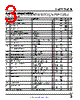
4 / 20 page  LT6274/LT6275 4 6275fa For more information www.linear.com/LT6275 Note 1: Stresses beyond those listed under Absolute Maximum Ratings may cause permanent damage to the device. Exposure to any Absolute Maximum Rating condition for extended periods may affect device reliability and lifetime. Note 2: Differential inputs of ±10V are appropriate for transient operation only, such as during slewing. Large, sustained differential inputs will cause excessive power dissipation and may damage the part. See Input Considerations in the Applications Information section of this data sheet for more details. Note 3: The inputs are protected by ESD protection diodes to each power supply. The Input current should be limited to less than 10mA. Note 4: A heat sink may be required to keep the junction temperature below the absolute maximum rating when the output is shorted indefinitely. Note 5: The LT6274I/LT6275I are guaranteed functional over the operating temperature range of –40°C to 85°C. The LT6274H/LT6275H are guaranteed functional over the operating temperature range of –40°C to 125°C. The l denotes the specifications which apply over the full operating temperature range, otherwise specifications are at TA = 25°C. Unless noted otherwise, VCM = 0V, and specifications apply at both VS = (V+ – V–) = ±5V and ±15V. SYMBOL PARAMETER CONDITIONS MIN TYP MAX UNITS tR, tF Small Signal Rise/Fall Time AV = 1, 10% – 90%, 100mV Input Step 4 ns tPD Propagation Delay 50% VIN to 50% VOUT, 100mV Input Step 4 ns ts Settling Time 1% of 10V Step, AV = 1, VS = ±15V 0.1% of 10V Step, AV = 1, VS = ±15V 1% of 5V Step, AV = 1, VS = ±5V 40 185 65 ns ns ns Note 6: The LT6274I/LT6275I are guaranteed to meet specified performance from –40°C to 85°C. The LT6274H/LT6275H are guaranteed to meet specified performance from –40°C to 125°C. Note 7: Input offset voltage is pulse tested and is exclusive of warm-up drift. Note 8: This parameter is not 100% tested. Note 9: Input voltage range is guaranteed by common mode rejection ratio test. Note 10: Supply voltage range is guaranteed by power supply rejection ratio test. Note 11: Slew rate is measured between 20% and 80% of output step with ±6V input (at AV = –2) and ±10V input (at AV = ±1) for ±15V supplies, and between 35% and 65% of output step with ±1.75V input (at AV = –2) for ±5V supplies. Note 12: Current density limitations within the IC require the continuous RMS current supplied by the output (sourcing or sinking) over the operating lifetime of the part be limited to under 115mA (Absolute Maximum). Proper heat sinking may be required to keep the junction temperature below the absolute maximum rating. ELECTRICAL CHARACTERISTICS |
|
|
Link URL |
| Cho đến nay ALLDATASHEET có giúp ích cho doanh nghiệp của bạn hay không? [ DONATE ] |
Alldatasheet là | Quảng cáo | Liên lạc với chúng tôi | Chính sách bảo mật | Liên kết đến bảng dữ liệu | Trao đổi link | Tìm kiếm theo nhà sản xuất All Rights Reserved©Alldatasheet.com |
| Russian : Alldatasheetru.com | Korean : Alldatasheet.co.kr | Spanish : Alldatasheet.es | French : Alldatasheet.fr | Italian : Alldatasheetit.com Portuguese : Alldatasheetpt.com | Polish : Alldatasheet.pl | Vietnamese : Alldatasheet.vn Indian : Alldatasheet.in | Mexican : Alldatasheet.com.mx | British : Alldatasheet.co.uk | New Zealand : Alldatasheet.co.nz |
|
Family Site : ic2ic.com |
icmetro.com |
 Vietnamese ▼
 English
 Chinese
 German
 Japanese
 Russian
 Korean
 Spanish
 French
 Italian
 Portuguese
 Polish
 Vietnamese
 Indian
 Mexican
 British
 New Zealand