 |
công cụ tìm kiếm bảng dữ liệu linh kiện điện tử |
|
|
công cụ tìm kiếm bảng dữ liệu linh kiện điện tử |
|
The question interval is too short.
Please try again in a few seconds.

Hello, Please ask a question about SN75LVDS82DGGR Datasheet
# Example questions:
➢ What is the typical supply current of the sn75lvds82 at a clock frequency of 50 mhz with a grayscale pattern?
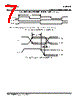
➢ What is the purpose of the 'receiver input skew margin' test, as illustrated in figure 7, and what parameter does it measure?
➢ How does zero-to-peak output jitter change with increasing modulation frequency when vcc = 3v and ta = 25°c?
| Part No. | SN75LVDS82DGGR |
| Manufacturer | TI |
| Size | 699 Kbytes |
| Pages | 18 pages |
| Description | FlatLink??RECEIVER |





# SN75LVDS82 FlatLink™ Receiver
## Features
️· 4:28 Data Channel Expansion (up to 238 Mbytes/s)
️· Suited for SVGA, XGA, or SXGA displays
️· Low EMI data transmission
️· Four Data Channels & Clock Differential Inputs
️· Operates from a single 3.3V supply (250mW typical)
️· 5V Tolerant Shutdown Input
️· Falling Clock-Edge Triggered Outputs
️· TSSOP Package (20-mil terminal pitch)
️· Low power consumption (<1mW when disabled)
️· Wide Phase-Lock Input Frequency Range (31 MHz to 68 MHz)
️· No external components required for PLL
️· Meets/Exceeds ANSI EIA/TIA-644 standards
️· Replacement for National™ DS90C582
## Description
The SN75LVDS82 integrates four serial-in, 7-bit parallel-out shift registers, a clock synthesizer, and five LVDS line receivers. It receives data from a transmitter (e.g., SN75LVDS81) over five balanced-pair conductors, expanding to 28 bits of single-ended LVTTL data. It can also be used with SN75LVDS84/85 for 21-bit transfers.
The device loads data into registers at the LVDS input clock rate (CLKIN) and outputs it on a 28-bit parallel bus at the same rate. A PLL generates a 7x clock for internal functions and the output clock (CLKOUT). Valid data is presented on the falling edge of CLKOUT.
## Functional Block Diagram
️· Includes: Serial-in/Parallel-out shift registers, clock synthesizer, LVDS receivers, and data bus.
## Absolute Maximum Ratings
️· VCC: -0.5V to 4V
️· Output Voltage: -0.5V to VCC + 0.5V
️· Input Voltage (all except SHTDN): -0.5V to VCC + 0.5V
️· SHTDN Input: -0.5V to 5.5V
️· Operating Temperature: 0°C to 70°C
️· Storage Temperature: -65°C to 150°C
## Electrical Characteristics
️· Positive-going differential input threshold voltage: 100 mV
️· High-level output voltage (IOH = -4 mA): 2.4 V
️· Low-level output voltage (IOL = 4 mA): 0.4 V
️· Quiescent current: 280 µA (disabled), 60-74 mA (enabled)
## Timing Requirements
️· Cycle time (input clock): 14.7 – 32.3 ns
️· Setup time: 600 ps
️· Hold time: 600 ps
## Package Information
️· Package Type: TSSOP
️· Pins: 56
# SN75LVDS82 FlatLink™ Receiver
## Features
️· 4:28 Data Channel Expansion (up to 238 Mbytes/s)
️· Suited for SVGA, XGA, or SXGA displays
️· Low EMI data transmission
️· Four Data Channels & Clock Differential Inputs
️· Operates from a single 3.3V supply (250mW typical)
️· 5V Tolerant Shutdown Input
️· Falling Clock-Edge Triggered Outputs
️· TSSOP Package (20-mil terminal pitch)
️· Low power consumption (<1mW when disabled)
️· Wide Phase-Lock Input Frequency Range (31 MHz to 68 MHz)
️· No external components required for PLL
️· Meets/Exceeds ANSI EIA/TIA-644 standards
️· Replacement for National™ DS90C582
## Description
The SN75LVDS82 integrates four serial-in, 7-bit parallel-out shift registers, a clock synthesizer, and five LVDS line receivers. It receives data from a transmitter (e.g., SN75LVDS81) over five balanced-pair conductors, expanding to 28 bits of single-ended LVTTL data. It can also be used with SN75LVDS84/85 for 21-bit transfers.
The device loads data into registers at the LVDS input clock rate (CLKIN) and outputs it on a 28-bit parallel bus at the same rate. A PLL generates a 7x clock for internal functions and the output clock (CLKOUT). Valid data is presented on the falling edge of CLKOUT.
## Functional Block Diagram
️· Includes: Serial-in/Parallel-out shift registers, clock synthesizer, LVDS receivers, and data bus.
## Absolute Maximum Ratings
️· VCC: -0.5V to 4V
️· Output Voltage: -0.5V to VCC + 0.5V
️· Input Voltage (all except SHTDN): -0.5V to VCC + 0.5V
️· SHTDN Input: -0.5V to 5.5V
️· Operating Temperature: 0°C to 70°C
️· Storage Temperature: -65°C to 150°C
## Electrical Characteristics
️· Positive-going differential input threshold voltage: 100 mV
️· High-level output voltage (IOH = -4 mA): 2.4 V
️· Low-level output voltage (IOL = 4 mA): 0.4 V
️· Quiescent current: 280 µA (disabled), 60-74 mA (enabled)
## Timing Requirements
️· Cycle time (input clock): 14.7 – 32.3 ns
️· Setup time: 600 ps
️· Hold time: 600 ps
## Package Information
️· Package Type: TSSOP
️· Pins: 56
| Part No. | SN75LVDS82DGGR |
| Manufacturer | TI |
| Size | 699 Kbytes |
| Pages | 18 pages |
| Description | FlatLink??RECEIVER |
| Cho đến nay ALLDATASHEET có giúp ích cho doanh nghiệp của bạn hay không? [ DONATE ] |
Alldatasheet là | Quảng cáo | Liên lạc với chúng tôi | Chính sách bảo mật | Liên kết đến bảng dữ liệu | Trao đổi link | Tìm kiếm theo nhà sản xuất All Rights Reserved©Alldatasheet.com |
| Russian : Alldatasheetru.com | Korean : Alldatasheet.co.kr | Spanish : Alldatasheet.es | French : Alldatasheet.fr | Italian : Alldatasheetit.com Portuguese : Alldatasheetpt.com | Polish : Alldatasheet.pl | Vietnamese : Alldatasheet.vn Indian : Alldatasheet.in | Mexican : Alldatasheet.com.mx | British : Alldatasheet.co.uk | New Zealand : Alldatasheet.co.nz |
|
Family Site : ic2ic.com |
icmetro.com |
 Vietnamese ▼
  English
 Chinese
 German
 Japanese
 Russian
 Korean
 Spanish
 French
 Italian
 Portuguese
 Polish
 Indian
 Mexican
 British
 New Zealand