 |
công cụ tìm kiếm bảng dữ liệu linh kiện điện tử |
|
|
công cụ tìm kiếm bảng dữ liệu linh kiện điện tử |
|
The question interval is too short.
Please try again in a few seconds.

Hello, Please ask a question about 2N7002BKS Datasheet
# Example questions:
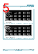
➢ What is the typical gate-source threshold voltage (vgs(th)) at an ambient temperature of 25°c, according to figure 12?
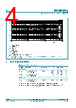
➢ What is the maximum height (he) of the package in millimeters?
➢ What happens to the drain current (id) as the gate-source voltage (vgs) increases, assuming a constant drain-source voltage (vds)?
| Part No. | 2N7002BKS |
| Manufacturer | NEXPERIA |
| Size | 931 Kbytes |
| Pages | 16 pages |
| Description | 60 V, 300 mA dual N-channel Trench MOSFET |

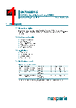






1. General Description:
️· Device: Nexperia 2N7002BKS
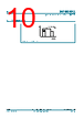
️· Type: N-channel MOSFET
️· Technology: TrenchMOS
️· Application: Suitable for various applications including DC-DC converters, load switches, and general-purpose switching.
2. Key Electrical Characteristics (at specified voltages/temperatures, unless otherwise noted):
️· V<sub>DS</sub> (Drain-Source Voltage): 60 V
️· V<sub>GS</sub> (Gate-Source Voltage): 20 V
️· R<sub>DS(on)</sub> (Drain-Source On-Resistance): Low (Specific values vary with V<sub>GS</sub> and temperature; see graphs)
️· I<sub>D</sub> (Drain Current): 300 mA (continuous)
️· Threshold Voltage (V<sub>GS(th)</sub>): Approximately 1V (Varies with temperature, see graph)
3. Detailed Specifications (Selected Highlights - Refer to the datasheet for complete values):
️· Absolute Maximum Ratings:
- Drain-Source Voltage (VDS): 60 V
- Gate-Source Voltage (VGS): 20 V
- Drain Current (continuous): 300 mA
- Power Dissipation: (See datasheet)
- Channel Temperature: 150 °C
️· Dynamic Characteristics:
- Input Capacitance (C<sub>iss</sub>): See datasheet graph
- Output Capacitance (C<sub>oss</sub>): See datasheet graph
- Reverse Transfer Capacitance (C<sub>rss</sub>): See datasheet graph
️· Thermal Characteristics:
- Thermal Resistance (Junction-to-Ambient): See datasheet
4. Electrical Characteristics (Selected Values):
| Parameter | Symbol | Test Conditions | Minimum/Typical/Maximum | Unit |
|---|---|---|---|---|
| Drain-Source Voltage | VDS | VGS = 0V | 60 | V |
| Gate-Source Voltage | VGS | VDS = 0V | 20 | V |
| Drain Current (continuous) | ID | VDS = 10V, VGS = 10V | 300 | mA |
| Drain-Source On-Resistance | RDS(on) | VGS = 10V, ID = 300 mA | Refer to Datasheet Graph | Ω |
| Gate-Source Threshold Voltage | VGS(th) | VDS = VGS, ID = 250µA | 1 | V |
1. General Description:
️· Device: Nexperia 2N7002BKS
️· Type: N-channel MOSFET
️· Technology: TrenchMOS
️· Application: Suitable for various applications including DC-DC converters, load switches, and general-purpose switching.
2. Key Electrical Characteristics (at specified voltages/temperatures, unless otherwise noted):
️· V<sub>DS</sub> (Drain-Source Voltage): 60 V
️· V<sub>GS</sub> (Gate-Source Voltage): 20 V
️· R<sub>DS(on)</sub> (Drain-Source On-Resistance): Low (Specific values vary with V<sub>GS</sub> and temperature; see graphs)
️· I<sub>D</sub> (Drain Current): 300 mA (continuous)
️· Threshold Voltage (V<sub>GS(th)</sub>): Approximately 1V (Varies with temperature, see graph)
3. Detailed Specifications (Selected Highlights - Refer to the datasheet for complete values):
️· Absolute Maximum Ratings:
- Drain-Source Voltage (VDS): 60 V
- Gate-Source Voltage (VGS): 20 V
- Drain Current (continuous): 300 mA
- Power Dissipation: (See datasheet)
- Channel Temperature: 150 °C
️· Dynamic Characteristics:
- Input Capacitance (C<sub>iss</sub>): See datasheet graph
- Output Capacitance (C<sub>oss</sub>): See datasheet graph
- Reverse Transfer Capacitance (C<sub>rss</sub>): See datasheet graph
️· Thermal Characteristics:
- Thermal Resistance (Junction-to-Ambient): See datasheet
4. Electrical Characteristics (Selected Values):
| Parameter | Symbol | Test Conditions | Minimum/Typical/Maximum | Unit |
|---|---|---|---|---|
| Drain-Source Voltage | VDS | VGS = 0V | 60 | V |
| Gate-Source Voltage | VGS | VDS = 0V | 20 | V |
| Drain Current (continuous) | ID | VDS = 10V, VGS = 10V | 300 | mA |
| Drain-Source On-Resistance | RDS(on) | VGS = 10V, ID = 300 mA | Refer to Datasheet Graph | Ω |
| Gate-Source Threshold Voltage | VGS(th) | VDS = VGS, ID = 250µA | 1 | V |
| Part No. | 2N7002BKS |
| Manufacturer | NEXPERIA |
| Size | 931 Kbytes |
| Pages | 16 pages |
| Description | 60 V, 300 mA dual N-channel Trench MOSFET |
| Cho đến nay ALLDATASHEET có giúp ích cho doanh nghiệp của bạn hay không? [ DONATE ] |
Alldatasheet là | Quảng cáo | Liên lạc với chúng tôi | Chính sách bảo mật | Liên kết đến bảng dữ liệu | Trao đổi link | Tìm kiếm theo nhà sản xuất All Rights Reserved©Alldatasheet.com |
| Russian : Alldatasheetru.com | Korean : Alldatasheet.co.kr | Spanish : Alldatasheet.es | French : Alldatasheet.fr | Italian : Alldatasheetit.com Portuguese : Alldatasheetpt.com | Polish : Alldatasheet.pl | Vietnamese : Alldatasheet.vn Indian : Alldatasheet.in | Mexican : Alldatasheet.com.mx | British : Alldatasheet.co.uk | New Zealand : Alldatasheet.co.nz |
|
Family Site : ic2ic.com |
icmetro.com |
 Vietnamese ▼
  English
 Chinese
 German
 Japanese
 Russian
 Korean
 Spanish
 French
 Italian
 Portuguese
 Polish
 Indian
 Mexican
 British
 New Zealand