|
công cụ tìm kiếm bảng dữ liệu linh kiện điện tử |
|
|
công cụ tìm kiếm bảng dữ liệu linh kiện điện tử |
|
SN74LS393D bảng dữ liệu(PDF) 3 Page - ON Semiconductor |
|
|
|||||||||||||||||||||||||||||
SN74LS393D bảng dữ liệu(HTML) 3 Page - ON Semiconductor |
|
|
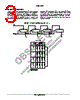
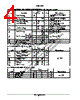
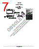
3 / 8 page  SN74LS393 http://onsemi.com 3 FUNCTIONAL DESCRIPTION Each half of the SN74LS393 operates in the Modulo 16 binary sequence, as indicated in the ÷16 Truth Table. The first flip-flop is triggered by HIGH-to-LOW transitions of the CP input signal. Each of the other flip-flops is triggered by a HIGH-to-LOW transition of the Q output of the preceding flip-flop. Thus state changes of the Q outputs do not occur simultaneously. This means that logic signals derived from combinations of these outputs will be subject to decoding spikes and, therefore, should not be used as clocks for other counters, registers or flip-flops. A HIGH signal on MR forces all outputs to the LOW state and prevents counting. SN74LS393 LOGIC DIAGRAM (one half shown) MR CP KCP J CD Q KCP J CD Q KCP J CD Q KCP J CD Q Q0 Q1 Q2 Q3 COUNT OUTPUTS Q3 Q2 Q1 Q0 0 1 2 3 4 5 6 7 8 9 10 11 L L L L H H H H H H H H L L H H L L H H L L H H L H L H L H L H L H L H L L L L L L L L H H H H 12 13 14 15 L L L L L L H H L H L H H H H H H = HIGH Voltage Level L = LOW Voltage Level TRUTH TABLE |
|
|
Link URL |
| Cho đến nay ALLDATASHEET có giúp ích cho doanh nghiệp của bạn hay không? [ DONATE ] |
Alldatasheet là | Quảng cáo | Liên lạc với chúng tôi | Chính sách bảo mật | Liên kết đến bảng dữ liệu | Trao đổi link | Tìm kiếm theo nhà sản xuất All Rights Reserved©Alldatasheet.com |
| Russian : Alldatasheetru.com | Korean : Alldatasheet.co.kr | Spanish : Alldatasheet.es | French : Alldatasheet.fr | Italian : Alldatasheetit.com Portuguese : Alldatasheetpt.com | Polish : Alldatasheet.pl | Vietnamese : Alldatasheet.vn Indian : Alldatasheet.in | Mexican : Alldatasheet.com.mx | British : Alldatasheet.co.uk | New Zealand : Alldatasheet.co.nz |
|
Family Site : ic2ic.com |
icmetro.com |
 Vietnamese ▼
 English
 Chinese
 German
 Japanese
 Russian
 Korean
 Spanish
 French
 Italian
 Portuguese
 Polish
 Vietnamese
 Indian
 Mexican
 British
 New Zealand