|
công cụ tìm kiếm bảng dữ liệu linh kiện điện tử |
|
|
công cụ tìm kiếm bảng dữ liệu linh kiện điện tử |
|
LT3653 bảng dữ liệu(PDF) 5 Page - Linear Technology |
|
|
|||||||||||||||||||||||||||||
LT3653 bảng dữ liệu(HTML) 5 Page - Linear Technology |
|
|
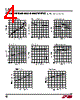
5 / 12 page  LT3653 5 3653f TYPICAL PERFORMANCE CHARACTERISTICS VC Current VC Operating Range PIN FUNCTIONS VIN (Pin 1): The VIN pin supplies current to the LT3653’s internal regulator and the internal power switch. Locally bypass this pin with a capacitor. HVOK (Pin 2): The HVOK pin is a status pin which indi- cates that the internal bias rail is present and that an input undervoltage lockout fault, an overvoltage lockout fault or an over temperature fault are not present. VC (Pin 3): The VC pin is the output of the internal error amplifier and is internally compensated. The voltage on this pin controls the peak switch current. Connect this pin to the battery charger VC pin for battery tracking function. ILIM (Pin 4): Connect a resistor to GND to program the output current limit of the regulator. See the ILIM Resistor section in Application Information. VOUT (Pin 5): The VOUT pin is connected to the negative terminal of the internal current sense resistor of the output current limit circuit. Maximum VOUT voltage is regulated to 4.8V. ISENSE (Pin 6): The ISENSE pin is the positive input to the internal current sense resistor of the output current limit circuit. The ISENSE pin is also the anode of the internal BOOST diode. BOOST (Pin 7): The BOOST pin provides a drive voltage, higher than the input voltage, to the internal power switch. The BOOST pin is internally connected to the cathode of the BOOST diode. SW (Pin 8): The SW pin is the output of the internal power switch. Connect this pin to the inductor, catch diode and boost capacitor. Exposed Pad (Pin 9): Ground. The Exposed Pad must be soldered to the PCB and electrically connected to ground. Use a large ground plane and vias to optimize thermal performance. VOUT (V) 15 10 3653 G09 –25 –20 –15 –10 –5 0 5 4 4.4 4.8 5.2 5.6 6 TEMPERATURE (ºC) 2.0 1.8 0.0 3653 G10 0.2 0.4 0.6 0.8 1.0 1.2 1.4 1.6 -50 -25 0 25 50 75 100 125 CURRENT LIMIT CLAMP SWITCHING THRESHOLD TA = 25°C unless otherwise noted |
|
|
Link URL |
| Cho đến nay ALLDATASHEET có giúp ích cho doanh nghiệp của bạn hay không? [ DONATE ] |
Alldatasheet là | Quảng cáo | Liên lạc với chúng tôi | Chính sách bảo mật | Liên kết đến bảng dữ liệu | Trao đổi link | Tìm kiếm theo nhà sản xuất All Rights Reserved©Alldatasheet.com |
| Russian : Alldatasheetru.com | Korean : Alldatasheet.co.kr | Spanish : Alldatasheet.es | French : Alldatasheet.fr | Italian : Alldatasheetit.com Portuguese : Alldatasheetpt.com | Polish : Alldatasheet.pl | Vietnamese : Alldatasheet.vn Indian : Alldatasheet.in | Mexican : Alldatasheet.com.mx | British : Alldatasheet.co.uk | New Zealand : Alldatasheet.co.nz |
|
Family Site : ic2ic.com |
icmetro.com |
 Vietnamese ▼
 English
 Chinese
 German
 Japanese
 Russian
 Korean
 Spanish
 French
 Italian
 Portuguese
 Polish
 Vietnamese
 Indian
 Mexican
 British
 New Zealand