|
công cụ tìm kiếm bảng dữ liệu linh kiện điện tử |
|
|
công cụ tìm kiếm bảng dữ liệu linh kiện điện tử |
|
ICS2510C bảng dữ liệu(PDF) 3 Page - Integrated Circuit Systems |
|
|
|||||||||||||||||||||||||||||
ICS2510C bảng dữ liệu(HTML) 3 Page - Integrated Circuit Systems |
|
|
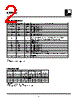
3 / 7 page  3 ICS2510C Absolute Maximum Ratings Supply Voltage (AVCC) . . . . . . . . . . . . . . . . . . . AVCC < (Vcc + 0.7V) Supply Voltage (VCC) . . . . . . . . . . . . . . . . . . . . 4.3 V Logic Inputs . . . . . . . . . . . . . . . . . . . . . . . . . . . . GND –0.5 V to Vcc +0.5 V Ambient Operating Temperature . . . . . . . . . . . . 0°C to +70°C Storage Temperature . . . . . . . . . . . . . . . . . . . . . . –65°C to +150°C Stresses above those listed under Absolute Maximum Ratings may cause permanent damage to the device. These ratings are stress specifications only and functional operation of the device at these or any other conditions above those listed in the operational sections of the specifications is not implied. Exposure to absolute maximum rating conditions for extended periods may affect product reliability. Electrical Characteristics - OUTPUT T A = 0 - 70C; VDD = VDDL = 3.3 V +/-10%; CL = 20 - 30 pF; RL = 470 Ohms (unless otherwise stated) PARAMETER SYMBOL CONDITIONS MIN TYP MAX UNITS Output Impedance R DSP V O = VDD*(0.5) 36 Ω Output Impedance R DSN V O = VDD*(0.5) 32 Ω Output High Voltage V OH I OH = -8 mA 2.4 2.9 V Output Low Voltage V OL I OL = 8 mA 0.25 0.4 V V OH = 2.4 V -26 -13.6 V OH = 2.0 V -37 -22 V OL = 0.8 V 19 25 V OL = 0.55 V 13 17 Rise Time 1 T r V OL = 0.8 V, VOH = 2.0 V 0.5 1.4 2.1 ns Fall Time 1 T f V OH = 2.0 V, VOL = 0.8 V 0.5 1.5 2.7 ns Duty Cycle 1 D t V T = 1.5 V;CL=30 pF 45 50 55 % at 66-100 MHz ; loaded outputs 52 100 at 133 MHz ; loaded outputs 39 75 Absolute Jitter 1 Tjabs 10000 cycles; C L = 30 pF 57 ps Skew 1 T sk V T = 1.5 V (Window) Output to Output 80 150 ps Phase error 1 T pe V T = Vdd/2; CLKIN-FBIN -150 40 150 ps Phase error Jitter 1 T pe 3 V T = Vdd/2; CLKIN-FBIN; Delay Jitter -50 35 50 ps Delay Input-Output 1 D R1 V T = 1.5 V; PLL_EN = 0 3.3 3.7 ns 1 Guaranteed by design, not 100% tested in production. Cycle to Cycle jitter 1 Tcyc-cyc ps Output High Current Output Low Current I OH I OL mA mA |
|
|
Link URL |
| Cho đến nay ALLDATASHEET có giúp ích cho doanh nghiệp của bạn hay không? [ DONATE ] |
Alldatasheet là | Quảng cáo | Liên lạc với chúng tôi | Chính sách bảo mật | Liên kết đến bảng dữ liệu | Trao đổi link | Tìm kiếm theo nhà sản xuất All Rights Reserved©Alldatasheet.com |
| Russian : Alldatasheetru.com | Korean : Alldatasheet.co.kr | Spanish : Alldatasheet.es | French : Alldatasheet.fr | Italian : Alldatasheetit.com Portuguese : Alldatasheetpt.com | Polish : Alldatasheet.pl | Vietnamese : Alldatasheet.vn Indian : Alldatasheet.in | Mexican : Alldatasheet.com.mx | British : Alldatasheet.co.uk | New Zealand : Alldatasheet.co.nz |
|
Family Site : ic2ic.com |
icmetro.com |
 Vietnamese ▼
 English
 Chinese
 German
 Japanese
 Russian
 Korean
 Spanish
 French
 Italian
 Portuguese
 Polish
 Vietnamese
 Indian
 Mexican
 British
 New Zealand