|
công cụ tìm kiếm bảng dữ liệu linh kiện điện tử |
|
|
công cụ tìm kiếm bảng dữ liệu linh kiện điện tử |
|
PIC18F4680ISPQTP bảng dữ liệu(PDF) 473 Page - Microchip Technology |
|
|
|||||||||||||||||||||||||||||
PIC18F4680ISPQTP bảng dữ liệu(HTML) 473 Page - Microchip Technology |
|
|
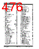
473 / 482 page  © 2007 Microchip Technology Inc. Preliminary DS39625C-page 471 PIC18F2585/2680/4585/4680 Pinout I/O Descriptions PIC18F2585/2680 ...................................................... 12 PIC18F4585/4680 ...................................................... 16 PIR Registers ................................................................... 118 PLL Use with INTOSC ....................................................... 25 PLL Frequency Multiplier ................................................... 25 HSPLL Oscillator Mode .............................................. 25 In INTOSC Modes ...................................................... 26 PLL Lock Time-out ............................................................. 45 POP ................................................................................. 390 POR. See Power-on Reset. PORTA Associated Registers ............................................... 131 I/O Summary ............................................................ 130 LATA Register .......................................................... 129 PORTA Register ...................................................... 129 TRISA Register ........................................................ 129 PORTB Associated Registers ............................................... 134 I/O Summary ............................................................ 133 LATB Register .......................................................... 132 PORTB Register ...................................................... 132 RB7:RB4 Interrupt-on-Change Flag (RBIF Bit) ......................................................... 132 TRISB Register ........................................................ 132 PORTC Associated Registers ............................................... 137 I/O Summary ............................................................ 136 LATC Register ......................................................... 135 PORTC Register ...................................................... 135 RC3/SCK/SCL Pin ................................................... 201 TRISC Register ........................................................ 135 PORTD Associated Registers ............................................... 140 I/O Summary ............................................................ 139 LATD Register ......................................................... 138 Parallel Slave Port (PSP) Function .......................... 138 PORTD Register ...................................................... 138 TRISD Register ........................................................ 138 PORTE Associated Registers ............................................... 143 I/O Summary ............................................................ 143 LATE Register .......................................................... 141 PORTE Register ...................................................... 141 PSP Mode Select (PSPMODE Bit) .......................... 138 TRISE Register ........................................................ 141 Postscaler, WDT Assignment (PSA Bit) .............................................. 149 Rate Select (T0PS2:T0PS0 Bits) ............................. 149 Switching Between Timer0 and WDT ...................... 149 Power Managed Modes ..................................................... 33 and A/D Operation ................................................... 254 and EUSART Operation ........................................... 231 and Multiple Sleep Commands .................................. 34 Clock Sources ............................................................ 33 Clock Transitions and Status Indicators ..................... 34 Effects on Clock Sources ........................................... 31 Entering ...................................................................... 33 Exiting Idle and Sleep Modes .................................... 39 by Interrupt ......................................................... 39 by Reset ............................................................. 39 by WDT Time-out ............................................... 39 Without an Oscillator Start-up Delay .................. 40 Idle Modes ................................................................. 37 PRI_IDLE .......................................................... 38 RC_IDLE ........................................................... 39 SEC_IDLE ......................................................... 38 Run Modes ................................................................ 34 PRI_RUN ........................................................... 34 RC_RUN ............................................................ 35 SEC_RUN ......................................................... 34 Selecting .................................................................... 33 Sleep Mode ............................................................... 37 Summary (table) ........................................................ 33 Power-on Reset (POR) ...................................................... 43 Oscillator Start-up Timer (OST) ................................. 45 Power-up Timer (PWRT) ........................................... 45 Time-out Sequence ................................................... 45 Power-up Delays ............................................................... 31 Power-up Timer (PWRT) ............................................. 31, 45 Prescaler Timer2 ..................................................................... 176 Prescaler, Capture ........................................................... 165 Prescaler, Timer0 ............................................................ 149 Assignment (PSA Bit) .............................................. 149 Rate Select (T0PS2:T0PS0 Bits) ............................. 149 Switching Between Timer0 and WDT ...................... 149 Prescaler, Timer2 ............................................................ 170 PRI_IDLE Mode ................................................................. 38 PRI_RUN Mode ................................................................. 34 Program Counter ............................................................... 62 PCL, PCH and PCU Registers .................................. 62 PCLATH and PCLATU Registers .............................. 62 Program Memory and the Extended Instruction Set .............................. 91 Code Protection ....................................................... 358 Instructions ................................................................ 66 Two-Word .......................................................... 66 Interrupt Vector .......................................................... 61 Look-up Tables .......................................................... 64 Map and Stack (diagram) .......................................... 61 Reset Vector .............................................................. 61 Program Verification and Code Protection ...................... 357 Associated Registers ............................................... 357 Programming, Device Instructions ................................... 361 PSP. See Parallel Slave Port. Pulse-Width Modulation. See PWM (CCP1 Module) and PWM (ECCP1 Module). PUSH ............................................................................... 390 PUSH and POP Instructions .............................................. 63 PUSHL ............................................................................. 406 PWM (CCP1 Module) ...................................................... 169 Associated Registers ............................................... 171 Duty Cycle ............................................................... 169 ECCPR1H:ECCPR1L Registers .............................. 169 Example Frequencies/Resolutions .......................... 170 Period ...................................................................... 169 Setup for PWM Operation ....................................... 170 TMR2 to PR2 Match ................................................ 169 PWM (ECCP1 Module) .................................................... 175 Associated Registers ............................................... 186 Auto-Shutdown ........................................................ 170 Direction Change in Full-Bridge Output Mode .................................................... 180 Duty Cycle ............................................................... 176 ECCPR1H:ECCPR1L Registers .............................. 175 Effects of a Reset .................................................... 185 Enhanced PWM Auto-Shutdown ............................. 182 |
|
Link URL |
| Cho đến nay ALLDATASHEET có giúp ích cho doanh nghiệp của bạn hay không? [ DONATE ] |
Alldatasheet là | Quảng cáo | Liên lạc với chúng tôi | Chính sách bảo mật | Liên kết đến bảng dữ liệu | Trao đổi link | Tìm kiếm theo nhà sản xuất All Rights Reserved©Alldatasheet.com |
| Russian : Alldatasheetru.com | Korean : Alldatasheet.co.kr | Spanish : Alldatasheet.es | French : Alldatasheet.fr | Italian : Alldatasheetit.com Portuguese : Alldatasheetpt.com | Polish : Alldatasheet.pl | Vietnamese : Alldatasheet.vn Indian : Alldatasheet.in | Mexican : Alldatasheet.com.mx | British : Alldatasheet.co.uk | New Zealand : Alldatasheet.co.nz |
|
Family Site : ic2ic.com |
icmetro.com |
 Vietnamese ▼
 English
 Chinese
 German
 Japanese
 Russian
 Korean
 Spanish
 French
 Italian
 Portuguese
 Polish
 Vietnamese
 Indian
 Mexican
 British
 New Zealand