|
công cụ tìm kiếm bảng dữ liệu linh kiện điện tử |
|
|
công cụ tìm kiếm bảng dữ liệu linh kiện điện tử |
|
OP196 bảng dữ liệu(PDF) 12 Page - Analog Devices |
|
|
|||||||||||||||||||||||||||||
OP196 bảng dữ liệu(HTML) 12 Page - Analog Devices |
|
|
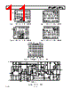
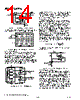
12 / 16 page  OP196/OP296/OP496 REV. B –12– APPLICATIONS INFORMATION Functional Description The OP196 family of operational amplifiers is comprised of single- supply, micropower, rail-to-rail input and output amplifiers. Input offset voltage (VOS) is only 300 µV maximum, while the output will deliver ±5 mA to a load. Supply current is only 50 µA, while bandwidth is over 450 kHz and slew rate is 0.3 V/ µs. Figure 36 is a simplified schematic of the OP196—it displays the novel circuit design techniques used to achieve this performance. Input Overvoltage Protection The OPx96 family of op amps uses a composite PNP/NPN input stage. Transistor Q1 in Figure 36 has a collector-base voltage of 0 V if +IN = VEE. If +IN then exceeds VEE, the junc- tion will be forward biased and large diode currents will flow, which may damage the device. The same situation applies to +IN on the base of transistor Q5 being driven above VCC. There- fore, the inverting and noninverting inputs must not be driven above or below either supply rail unless the input current is limited. Figure 37 shows the input characteristics for the OPx96 family. This photograph was generated with the power supply pins connected to ground and a curve tracer’s collector output drive connected to the input. As shown in the figure, when the input voltage exceeds either supply by more than 0.6 V, internal pn- junctions energize and permit current flow from the inputs to the supplies. If the current is not limited, the amplifier may be damaged. To prevent damage, the input current should be limited to no more than 5 mA. 10 0% 100 90 8 6 4 2 0 –2 –4 –6 –8 –1.5 –1 –0.5 0 0.5 1 1.5 INPUT VOLTAGE – Volts Figure 37. Input Overvoltage I-V Characteristics of the OPx96 Family Output Phase Reversal Some other operational amplifiers designed for single-supply operation exhibit an output voltage phase reversal when their inputs are driven beyond their useful common-mode range. Typically for single-supply bipolar op amps, the negative supply determines the lower limit of their common-mode range. With these common-mode limited devices, external clamping diodes are required to prevent input signal excursions from exceeding the device’s negative supply rail (i.e., GND) and triggering output phase reversal. The OPx96 family of op amps is free from output phase reversal effects due to its novel input structure. Figure 38 illustrates the performance of the OPx96 op amps when the input is driven beyond the supply rails. As previously mentioned, amplifier input current must be limited if the inputs are driven beyond the supply rails. In the circuit of Figure 38, the source amplitude is ±15 V, while the supply voltage is only ±5 V. In this case, a 2 k Ω source resistor limits the input current to 5 mA. 10 0% 100 90 VS = 5V AV = 1 5V 1ms 5V 0 0 VIN VOUT TIME – 1ns/DIV Figure 38. Output Voltage Phase Reversal Behavior Input Offset Voltage Nulling The OP196 provides two offset adjust terminals that can be used to null the amplifier’s internal VOS. In general, operational amplifier terminals should never be used to adjust system offset voltages. A 100 k Ω potentiometer, connected as shown in Fig- ure 39, is recommended to null the OP196’s offset voltage. Offset nulling does not adversely affect TCVOS performance, providing that the trimming potentiometer temperature coeffi- cient does not exceed ±100 ppm/°C. 6 7 2 3 V– V+ OP196 100k 4 1 5 Figure 39. Offset Nulling Circuit Driving Capacitive Loads OP196 family amplifiers are unconditionally stable with capaci- tive loads less than 170 pF. When driving large capacitive loads in unity-gain configurations, an in-the-loop compensation technique is recommended, as illustrated in Figure 40. OP296 CF VIN RG RF RX CL VOUT RX = WHERE RO = OPEN-LOOP OUTPUT RESISTANCE RO RG RF CF = I + ( ) ( ) C L RO I | ACL| RF + RG RF Figure 40. In-the-Loop Compensation Technique for Driving Capacitive Loads |
|
|
Link URL |
| Cho đến nay ALLDATASHEET có giúp ích cho doanh nghiệp của bạn hay không? [ DONATE ] |
Alldatasheet là | Quảng cáo | Liên lạc với chúng tôi | Chính sách bảo mật | Liên kết đến bảng dữ liệu | Trao đổi link | Tìm kiếm theo nhà sản xuất All Rights Reserved©Alldatasheet.com |
| Russian : Alldatasheetru.com | Korean : Alldatasheet.co.kr | Spanish : Alldatasheet.es | French : Alldatasheet.fr | Italian : Alldatasheetit.com Portuguese : Alldatasheetpt.com | Polish : Alldatasheet.pl | Vietnamese : Alldatasheet.vn Indian : Alldatasheet.in | Mexican : Alldatasheet.com.mx | British : Alldatasheet.co.uk | New Zealand : Alldatasheet.co.nz |
|
Family Site : ic2ic.com |
icmetro.com |
 Vietnamese ▼
 English
 Chinese
 German
 Japanese
 Russian
 Korean
 Spanish
 French
 Italian
 Portuguese
 Polish
 Vietnamese
 Indian
 Mexican
 British
 New Zealand