|
công cụ tìm kiếm bảng dữ liệu linh kiện điện tử |
|
|
công cụ tìm kiếm bảng dữ liệu linh kiện điện tử |
|
ADA4432-1BCPZ-R2 bảng dữ liệu(PDF) 6 Page - Analog Devices |
|
|
|||||||||||||||||||||||||||||
ADA4432-1BCPZ-R2 bảng dữ liệu(HTML) 6 Page - Analog Devices |
|
|
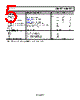
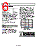
6 / 28 page  ADA4432-1/ADA4433-1 Data Sheet Rev. A | Page 6 of 28 ABSOLUTE MAXIMUM RATINGS Table 3. Parameter Rating Supply Voltage 4 V Output Common-Mode Voltage 22 V Input Differential Voltage +VS Power Dissipation See Figure 3 Storage Temperature Range −65°C to +125°C Operating Temperature Range −40°C to +125°C Lead Temperature (Soldering, 10 sec) 260°C Junction Temperature 150°C Stresses above those listed under Absolute Maximum Ratings may cause permanent damage to the device. This is a stress rating only; functional operation of the device at these or any other conditions above those indicated in the operational section of this specification is not implied. Exposure to absolute maximum rating conditions for extended periods may affect device reliability. THERMAL RESISTANCE θJA is specified for the device soldered to a high thermal conductivity 4-layer (2s2p) circuit board, as described in EIA/JESD 51-7. Table 4. Package Type θJA θJC Unit 6-Lead SOT-23 170 Not applicable °C/W 8-Lead LFCSP 50 5 °C/W MAXIMUM POWER DISSIPATION The maximum safe power dissipation in the ADA4432-1 and ADA4433-1 packages are limited by the associated rise in junction temperature (TJ) on the die. At approximately 150°C, which is the glass transition temperature, the plastic changes its properties. Exceeding a junction temperature of 150°C for an extended time can result in changes in the silicon devices, potentially causing failure. The power dissipated in the package (PD) is the sum of the quiescent power dissipation and the power dissipated in the package due to the load drive for all outputs. The quiescent power is the voltage between the supply pins (VS) times the quiescent current (IS). The power dissipated due to the load drive depends on the particular application. For each output, the power due to load drive is calculated by multiplying the load current by the associated voltage drop across the device. The power dissipated due to the loads is equal to the sum of the power dissipations due to each individual load. RMS voltages and currents must be used in these calculations. Airflow increases heat dissipation, effectively reducing θJA. Figure 3 shows the maximum power dissipation in the package vs. the ambient temperature for the 6-lead SOT-23 (170°C/W) and the 8-lead LFCSP (50°C/W) on a JEDEC standard 4-layer board. θJA values are approximate. Figure 3. Maximum Power Dissipation vs. Ambient Temperature for a 4-Layer Board ESD CAUTION 0 1 2 3 4 5 –40 –20 0 20 40 60 80 100 120 AMBIENT TEMPERATURE (ºC) TJ = 150°C LFCSP SOT-23 |
|
Link URL |
| Cho đến nay ALLDATASHEET có giúp ích cho doanh nghiệp của bạn hay không? [ DONATE ] |
Alldatasheet là | Quảng cáo | Liên lạc với chúng tôi | Chính sách bảo mật | Liên kết đến bảng dữ liệu | Trao đổi link | Tìm kiếm theo nhà sản xuất All Rights Reserved©Alldatasheet.com |
| Russian : Alldatasheetru.com | Korean : Alldatasheet.co.kr | Spanish : Alldatasheet.es | French : Alldatasheet.fr | Italian : Alldatasheetit.com Portuguese : Alldatasheetpt.com | Polish : Alldatasheet.pl | Vietnamese : Alldatasheet.vn Indian : Alldatasheet.in | Mexican : Alldatasheet.com.mx | British : Alldatasheet.co.uk | New Zealand : Alldatasheet.co.nz |
|
Family Site : ic2ic.com |
icmetro.com |
 Vietnamese ▼
 English
 Chinese
 German
 Japanese
 Russian
 Korean
 Spanish
 French
 Italian
 Portuguese
 Polish
 Vietnamese
 Indian
 Mexican
 British
 New Zealand