|
công cụ tìm kiếm bảng dữ liệu linh kiện điện tử |
|
|
công cụ tìm kiếm bảng dữ liệu linh kiện điện tử |
|
H8/3003 bảng dữ liệu(PDF) 711 Page - Renesas Technology Corp |
|
|
|||||||||||||||||||||||||||||
H8/3003 bảng dữ liệu(HTML) 711 Page - Renesas Technology Corp |
|
|
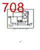
711 / 715 page  D.2 Pin States at Reset Reset in T1 State: Figure D-1 is a timing diagram for the case in which RES goes low during the T1 state of an external memory access cycle. As soon as RES goes low, all ports are initialized to the input state. AS, RD, HWR, and LWR go high, and the data bus goes to the high-impedance state. The address bus is initialized to the low output level 0.5 state after the low level of RES is sampled. Sampling of RES takes place at the fall of the system clock (ø). Figure D-1 Reset during Memory Access (Reset during T1 State) Access to external address ø Address bus CS CS to CS AS RD (read access) HWR, LWR Data bus I/O port 0 71 RES (write access) (write access) H'000000 High impedance High impedance High impedance High High High Internal reset signal T1 T2 T3 693 |
|
Link URL |
| Cho đến nay ALLDATASHEET có giúp ích cho doanh nghiệp của bạn hay không? [ DONATE ] |
Alldatasheet là | Quảng cáo | Liên lạc với chúng tôi | Chính sách bảo mật | Liên kết đến bảng dữ liệu | Trao đổi link | Tìm kiếm theo nhà sản xuất All Rights Reserved©Alldatasheet.com |
| Russian : Alldatasheetru.com | Korean : Alldatasheet.co.kr | Spanish : Alldatasheet.es | French : Alldatasheet.fr | Italian : Alldatasheetit.com Portuguese : Alldatasheetpt.com | Polish : Alldatasheet.pl | Vietnamese : Alldatasheet.vn Indian : Alldatasheet.in | Mexican : Alldatasheet.com.mx | British : Alldatasheet.co.uk | New Zealand : Alldatasheet.co.nz |
|
Family Site : ic2ic.com |
icmetro.com |
 Vietnamese ▼
 English
 Chinese
 German
 Japanese
 Russian
 Korean
 Spanish
 French
 Italian
 Portuguese
 Polish
 Vietnamese
 Indian
 Mexican
 British
 New Zealand