|
công cụ tìm kiếm bảng dữ liệu linh kiện điện tử |
|
|
công cụ tìm kiếm bảng dữ liệu linh kiện điện tử |
|
H8SX/1663M bảng dữ liệu(PDF) 680 Page - Renesas Technology Corp |
|
|
|||||||||||||||||||||||||||||
H8SX/1663M bảng dữ liệu(HTML) 680 Page - Renesas Technology Corp |
|
|
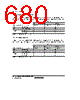
680 / 1504 page  Section 13 I/O Ports Rev. 2.00 Sep. 24, 2008 Page 648 of 1468 REJ09B0412-0200 (3) PK5/PO29/TIOCA10/TIOCB10 The pin function is switched as shown below according to the combination of register setting of PPG and TPU, setting of the port function control register (PFCR), and the PK5DDR bit settings. Setting PPG TPU I/O Port Module Name Pin Function PO29_OE TIOCB10_OE PK5DDR PPG PO29 output* 1 TPU TIOCB10 output* 0 1 PK5 output* 0 0 1 I/O port PK5 input* 0 0 0 Note: * Valid when PCJKE = 1. (4) PK4/PO28/TIOCA10 The pin function is switched as shown below according to the combination of register setting of PPG and TPU, setting of the port function control register (PFCR), and the PK4DDR bit settings. Setting PPG TPU I/O Port Module Name Pin Function PO28_OE TIOCA10_OE PK4DDR PPG PO28 output* 1 TPU TIOCA10 output* 0 1 PK4 output* 0 0 1 I/O port PK4 input* 0 0 0 Note: * Valid when PCJKE = 1. |
|
Link URL |
| Cho đến nay ALLDATASHEET có giúp ích cho doanh nghiệp của bạn hay không? [ DONATE ] |
Alldatasheet là | Quảng cáo | Liên lạc với chúng tôi | Chính sách bảo mật | Liên kết đến bảng dữ liệu | Trao đổi link | Tìm kiếm theo nhà sản xuất All Rights Reserved©Alldatasheet.com |
| Russian : Alldatasheetru.com | Korean : Alldatasheet.co.kr | Spanish : Alldatasheet.es | French : Alldatasheet.fr | Italian : Alldatasheetit.com Portuguese : Alldatasheetpt.com | Polish : Alldatasheet.pl | Vietnamese : Alldatasheet.vn Indian : Alldatasheet.in | Mexican : Alldatasheet.com.mx | British : Alldatasheet.co.uk | New Zealand : Alldatasheet.co.nz |
|
Family Site : ic2ic.com |
icmetro.com |
 Vietnamese ▼
 English
 Chinese
 German
 Japanese
 Russian
 Korean
 Spanish
 French
 Italian
 Portuguese
 Polish
 Vietnamese
 Indian
 Mexican
 British
 New Zealand