|
công cụ tìm kiếm bảng dữ liệu linh kiện điện tử |
|
|
công cụ tìm kiếm bảng dữ liệu linh kiện điện tử |
|
H8SX/1663R bảng dữ liệu(PDF) 373 Page - Renesas Technology Corp |
|
|
|||||||||||||||||||||||||||||
H8SX/1663R bảng dữ liệu(HTML) 373 Page - Renesas Technology Corp |
|
|
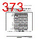
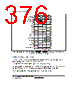
373 / 1504 page  Section 9 Bus Controller (BSC) Rev. 2.00 Sep. 24, 2008 Page 341 of 1468 REJ09B0412-0200 (3) When TRWL = 1 When the SDRAM interface is written to, one Trwl cycle is inserted after the Tc2 cycle. The DACK and EDACK signals stay asserted until the end of the Trwl cycle. The hold time of data output from an external device can be extended by one cycle. Figure 9.87 shows an output timing example of the DACK and EDACK signals when TRWL = 1 with DDS = 1, EDDS = 1, DKC = 0 and EDKC = 0. T p T r T c1 T c2 T rwl T c1 T c2 T rwl SDRAM φ Address bus Row address Column address 2 Column address 1 CS Precharge-sel RAS CAS WE CKE PALL ACTV NOP NOP WRIT WRIT NOP DQMLU DQMLL D7 to D0 BS DACK or EDACK RD/ WR D15 to D8 Row address High Figure 9.87 Output Timing Example of DACK and EDACK when TRWL = 1 (Write) |
|
Link URL |
| Cho đến nay ALLDATASHEET có giúp ích cho doanh nghiệp của bạn hay không? [ DONATE ] |
Alldatasheet là | Quảng cáo | Liên lạc với chúng tôi | Chính sách bảo mật | Liên kết đến bảng dữ liệu | Trao đổi link | Tìm kiếm theo nhà sản xuất All Rights Reserved©Alldatasheet.com |
| Russian : Alldatasheetru.com | Korean : Alldatasheet.co.kr | Spanish : Alldatasheet.es | French : Alldatasheet.fr | Italian : Alldatasheetit.com Portuguese : Alldatasheetpt.com | Polish : Alldatasheet.pl | Vietnamese : Alldatasheet.vn Indian : Alldatasheet.in | Mexican : Alldatasheet.com.mx | British : Alldatasheet.co.uk | New Zealand : Alldatasheet.co.nz |
|
Family Site : ic2ic.com |
icmetro.com |
 Vietnamese ▼
 English
 Chinese
 German
 Japanese
 Russian
 Korean
 Spanish
 French
 Italian
 Portuguese
 Polish
 Vietnamese
 Indian
 Mexican
 British
 New Zealand