|
công cụ tìm kiếm bảng dữ liệu linh kiện điện tử |
|
|
công cụ tìm kiếm bảng dữ liệu linh kiện điện tử |
|
H8S/2112 bảng dữ liệu(PDF) 709 Page - Renesas Technology Corp |
|
|
|||||||||||||||||||||||||||||
H8S/2112 bảng dữ liệu(HTML) 709 Page - Renesas Technology Corp |
|
|
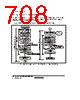
709 / 894 page  Section 22 Flash Memory Rev. 1.00 Mar. 18, 2008 Page 685 of 866 REJ09B0451-0100 The difference between the erasing procedures in user program mode and user boot mode depends on whether the MAT is switched or not as shown in figure 22.15. MAT switching is enabled by writing a specific value to FMATS. Note, however, that while the MATs are being switched, the LSI is in an unstable state, e.g. access to a MAT is not allowed until MAT switching is completed, and if an interrupt occurs, from which MAT the interrupt vector is read is undetermined. Perform MAT switching in accordance with the description in section 22.10, Switching between User MAT and User Boot MAT. Except for MAT switching, the erasing procedure is the same as that in user program mode. The area that can be executed in the steps of the user procedure program (on-chip RAM and user MAT) is shown in section 22.8.4, Storable Areas for On-Chip Program and Program Data. 22.8.4 Storable Areas for On-Chip Program and Program Data In the descriptions in this manual, the on-chip programs and program data storage areas are assumed to be in the on-chip RAM. However, they can be executed from part of the flash memory which is not to be programmed or erased as long as the following conditions are satisfied. • The on-chip program is downloaded to and executed in the on-chip RAM specified by FTDAR. Therefore, this on-chip RAM area is not available for use. • Since the on-chip program uses a stack area, allocate 128 bytes at the maximum as a stack area. • Download requested by setting the SCO bit in FCCS to 1 should be executed from the on-chip RAM because it will require switching of the memory MATs. • In an operating mode in which the external address space is not accessible, such as single-chip mode, the required procedure programs, NMI handling vector table, and NMI handling routine should be transferred to the on-chip RAM before programming/erasing starts (download result is determined). • The flash memory is not accessible during programming/erasing. Programming/erasing is executed by the program downloaded to the on-chip RAM. Therefore, the procedure program that initiates operation, the NMI handling vector table, and the NMI handling routine should be stored in the on-chip RAM other than the flash memory. • After programming/erasing starts, access to the flash memory should be inhibited until FKEY is cleared. The reset input state (period of RES = 0) must be set to at least 100 µs when the operating mode is changed and the reset start executed on completion of programming/erasing. Transitions to the reset state are inhibited during programming/erasing. When the reset signal is input, a reset input state (period of RES = 0) of at least 100 µs is needed before the reset signal is released. |
|
Link URL |
| Cho đến nay ALLDATASHEET có giúp ích cho doanh nghiệp của bạn hay không? [ DONATE ] |
Alldatasheet là | Quảng cáo | Liên lạc với chúng tôi | Chính sách bảo mật | Liên kết đến bảng dữ liệu | Trao đổi link | Tìm kiếm theo nhà sản xuất All Rights Reserved©Alldatasheet.com |
| Russian : Alldatasheetru.com | Korean : Alldatasheet.co.kr | Spanish : Alldatasheet.es | French : Alldatasheet.fr | Italian : Alldatasheetit.com Portuguese : Alldatasheetpt.com | Polish : Alldatasheet.pl | Vietnamese : Alldatasheet.vn Indian : Alldatasheet.in | Mexican : Alldatasheet.com.mx | British : Alldatasheet.co.uk | New Zealand : Alldatasheet.co.nz |
|
Family Site : ic2ic.com |
icmetro.com |
 Vietnamese ▼
 English
 Chinese
 German
 Japanese
 Russian
 Korean
 Spanish
 French
 Italian
 Portuguese
 Polish
 Vietnamese
 Indian
 Mexican
 British
 New Zealand