|
công cụ tìm kiếm bảng dữ liệu linh kiện điện tử |
|
|
công cụ tìm kiếm bảng dữ liệu linh kiện điện tử |
|
AD8341 bảng dữ liệu(PDF) 11 Page - Analog Devices |
|
|
|||||||||||||||||||||||||||||
AD8341 bảng dữ liệu(HTML) 11 Page - Analog Devices |
|
|
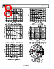
11 / 20 page  Data Sheet AD8341 Rev. B | Page 11 of 20 I-Q ATTENUATORS AND BASEBAND AMPLIFIERS The proprietary linear-responding attenuator structure is an active solution with differential inputs and outputs that offer excellent linearity, low noise, and greater immunity from mismatches than other variable attenuator methods. The gain, in linear terms, of the I and Q channels is proportional to its control voltage with a scaling factor designed to be 2/V, i.e., a full-scale gain setpoint of 1.0 (−4.5 dB) for a VBBI (or a VBBQ) of 500 mV. The control voltages can be driven differentially or single-ended. The combination of the baseband amplifiers and attenuators allows for maximum modulation bandwidths in excess of 200 MHz. OUTPUT AMPLIFIER The output amplifier accepts the sum of the attenuator outputs and delivers a differential output signal into the external load. The output pins must be pulled up to an external supply, preferably through RF chokes. When the 50 Ω load is taken differentially, an output P1dB and IP3 of 8.5 dBm and 17.5 dBm is achieved, respectively, at 1.9 GHz. The output can be taken in single-ended fashion, albeit at lower performance levels. NOISE AND DISTORTION The output noise floor and distortion levels vary with the gain magnitude but do not vary significantly with the phase. At the higher gain magnitude setpoints, the OIP3 and the noise floor vary in direct proportion with the gain. At lower gain magnitude setpoints, the noise floor levels off while the OIP3 continues to vary with the gain. GAIN AND PHASE ACCURACY There are numerous ways to express the accuracy of the AD8341. Ideally, the gain and phase must precisely follow the setpoints. Figure 4 illustrates the gain error in dB from a best fit line, normalized to the gain measured at the gain setpoint = 1.0, for the different phase setpoints. Figure 6 shows the gain error in a different form, normalized to the gain measured at phase setpoint = 0°; the phase setpoint is swept from 0° to 360° for different gain setpoints. Figure 8 and Figure 22 show analogous errors for the phase error as a function of gain and phase setpoints. The accuracy clearly depends on the region of operation within the vector gain unit circle. Operation very close to the origin generally results in larger errors as the relative accuracy of the I and Q vectors degrades. RF FREQUENCY RANGE The frequency range on the RF input is limited by the internal polyphase quadrature phase-splitter. The phase-splitter splits the incoming RF input into two signals, 90° out of phase, as previously described in the RF Quadrature Generator section. This polyphase network has been designed to ensure robust quadrature accuracy over standard fabrication process parameter variations for the 1.5 GHz to 2.4 GHz specified RF frequency range. Using the AD8341 as a single-sideband modulator and measuring the resul-ting sideband suppression is a good gauge of how well the quadrature accuracy is maintained over RF frequency. A typical plot of sideband suppression from 1.1 GHz to 2.7 GHz is shown in Figure 28. The level of sideband suppression degradation outside the 1.5 GHz to 2.4 GHz specified range is subject to manufacturing process variations. –15 –20 –45 –40 –35 –30 –25 0.7 2.7 2.5 2.3 2.1 1.9 1.7 1.5 1.3 0.9 1.1 FREQUENCY (GHz) Figure 28. Sideband Suppression vs. Frequency |
|
|
Link URL |
| Cho đến nay ALLDATASHEET có giúp ích cho doanh nghiệp của bạn hay không? [ DONATE ] |
Alldatasheet là | Quảng cáo | Liên lạc với chúng tôi | Chính sách bảo mật | Liên kết đến bảng dữ liệu | Trao đổi link | Tìm kiếm theo nhà sản xuất All Rights Reserved©Alldatasheet.com |
| Russian : Alldatasheetru.com | Korean : Alldatasheet.co.kr | Spanish : Alldatasheet.es | French : Alldatasheet.fr | Italian : Alldatasheetit.com Portuguese : Alldatasheetpt.com | Polish : Alldatasheet.pl | Vietnamese : Alldatasheet.vn Indian : Alldatasheet.in | Mexican : Alldatasheet.com.mx | British : Alldatasheet.co.uk | New Zealand : Alldatasheet.co.nz |
|
Family Site : ic2ic.com |
icmetro.com |
 Vietnamese ▼
 English
 Chinese
 German
 Japanese
 Russian
 Korean
 Spanish
 French
 Italian
 Portuguese
 Polish
 Vietnamese
 Indian
 Mexican
 British
 New Zealand