|
công cụ tìm kiếm bảng dữ liệu linh kiện điện tử |
|
|
công cụ tìm kiếm bảng dữ liệu linh kiện điện tử |
|
ADRF5702BCCZN-R7 bảng dữ liệu(PDF) 24 Page - Analog Devices |
|
|
|||||||||||||||||||||||||||||
ADRF5702BCCZN-R7 bảng dữ liệu(HTML) 24 Page - Analog Devices |
|
|
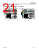
24 / 27 page  Data Sheet ADRF5702 THEORY OF OPERATION analog.com Rev. A | 24 of 27 SERIAL OR PARALLEL MODE SELECTION The ADRF5702 can be controlled in either serial or parallel mode by setting the PS pin to high or low, respectively (see Table 9). Table 9. Mode Selection PS Control Mode Low Parallel High Serial SERIAL MODE INTERFACE The ADRF5702 supports a 4-wire serial peripheral interface (SPI): serial data input (SERIN), clock (CLK), serial data output (SE- ROUT), and latch enable (LE). The serial control interface is acti- vated when the PS pin is set to high. The ADRF5702 attenuation states can be controlled using the 8-bit SERIN data. In serial mode, the SERIN data is clocked MSB first on the rising CLK edges into the shift register. Then, LE must be toggled high to latch the new attenuation state into the device. LE must be set to low to clock the new SERIN data into the shift register as CLK is masked to prevent the attenuator value from changing if LE is kept high. See Figure 53, Figure 54, the Timing Specifications section, and the RF Input and Output section for additional information. Figure 53. Serial Control Timing Diagram Figure 54. Serial Output Timing Diagram |
|
Link URL |
| Cho đến nay ALLDATASHEET có giúp ích cho doanh nghiệp của bạn hay không? [ DONATE ] |
Alldatasheet là | Quảng cáo | Liên lạc với chúng tôi | Chính sách bảo mật | Liên kết đến bảng dữ liệu | Trao đổi link | Tìm kiếm theo nhà sản xuất All Rights Reserved©Alldatasheet.com |
| Russian : Alldatasheetru.com | Korean : Alldatasheet.co.kr | Spanish : Alldatasheet.es | French : Alldatasheet.fr | Italian : Alldatasheetit.com Portuguese : Alldatasheetpt.com | Polish : Alldatasheet.pl | Vietnamese : Alldatasheet.vn Indian : Alldatasheet.in | Mexican : Alldatasheet.com.mx | British : Alldatasheet.co.uk | New Zealand : Alldatasheet.co.nz |
|
Family Site : ic2ic.com |
icmetro.com |
 Vietnamese ▼
 English
 Chinese
 German
 Japanese
 Russian
 Korean
 Spanish
 French
 Italian
 Portuguese
 Polish
 Vietnamese
 Indian
 Mexican
 British
 New Zealand