|
công cụ tìm kiếm bảng dữ liệu linh kiện điện tử |
|
|
công cụ tìm kiếm bảng dữ liệu linh kiện điện tử |
|
ADL8113ACCZ-R7 bảng dữ liệu(PDF) 1 Page - Analog Devices |
|
|
|||||||||||||||||||||||||||||
ADL8113ACCZ-R7 bảng dữ liệu(HTML) 1 Page - Analog Devices |
|
|
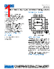
1 / 37 page  Data Sheet ADL8113 10MHz to 12GHz Low Noise Amplifier with 10MHz to 14GHz Bypass Switches Rev. 0 DOCUMENT FEEDBACK TECHNICAL SUPPORT Information furnished by Analog Devices is believed to be accurate and reliable "as is". However, no responsibility is assumed by Analog Devices for its use, nor for any infringements of patents or other rights of third parties that may result from its use. Specifications subject to change without notice. No license is granted by implication or otherwise under any patent or patent rights of Analog Devices. Trademarks and registered trademarks are the property of their respective owners. All Analog Devices products contained herein are subject to release and availability. FEATURES ► Wideband amplifier with multiple bypass modes ► 4 pin-selectable operating modes ► Internal amplifier mode operating from 10MHz to 12GHz ► Internal bypass mode operating from 10MHz to 14GHz ► Two external bypass modes from 10MHz to 14GHz ► Integrated power-supply decoupling ► Reflective bypass switches ► In internal amplifier mode ► Small signal gain: 14.0dB typical from 200MHz to 6GHz ► OP1dB: 20.5dBm typical from 200MHz to 6GHz ► OIP3: 35.5dBm typical from 200MHz to 6GHz ► OIP2: 44.6dBm typical from 9GHz to 12GHz ► Noise figure: 3.8dB typical from 200MHz to 6GHz ► In internal bypass switch mode ► Insertion loss: 2.2dB typical from 200MHz to 6GHz ► Operating temperature range: −40°C to +85°C ► RoHS-compliant, 6mm × 6mm, 28-terminal LGA APPLICATIONS ► Electronic test and measurement equipment ► Electronic warfare ► Wireless receivers FUNCTIONAL BLOCK DIAGRAM Figure 1. Functional Block Diagram GENERAL DESCRIPTION The ADL8113 is a low noise amplifier (LNA) with bypass switches that provides broadband operation from 10MHz to 12GHz. The ADL8113 provides a low noise figure of 3.8dB and an output third- order intercept point (OIP3) of 35.5dBm from 200MHz to 6GHz. The ADL8113 provides a small signal gain of 14.0dB that is stable over frequency, temperature, power supply, and from device to device. The integration of an amplifier and two SP4T reflective switches allows multiple paths through the device. The addition of switches also offers a high input third-order intercept (IIP3) path when large input signals are present. With the integration of power-supply decoupling capacitors, minimal external power-supply decoupling is required. The ADL8113 is fully specified for operation across a temperature range of −40°C to +85°C. The ADL8113 is available in a 6mm × 6mm, 28-terminal land grid array (LGA) package. |
Số phần tương tự - ADL8113ACCZ-R7 |
|
Mô tả tương tự - ADL8113ACCZ-R7 |
|
|
Link URL |
| Cho đến nay ALLDATASHEET có giúp ích cho doanh nghiệp của bạn hay không? [ DONATE ] |
Alldatasheet là | Quảng cáo | Liên lạc với chúng tôi | Chính sách bảo mật | Liên kết đến bảng dữ liệu | Trao đổi link | Tìm kiếm theo nhà sản xuất All Rights Reserved©Alldatasheet.com |
| Russian : Alldatasheetru.com | Korean : Alldatasheet.co.kr | Spanish : Alldatasheet.es | French : Alldatasheet.fr | Italian : Alldatasheetit.com Portuguese : Alldatasheetpt.com | Polish : Alldatasheet.pl | Vietnamese : Alldatasheet.vn Indian : Alldatasheet.in | Mexican : Alldatasheet.com.mx | British : Alldatasheet.co.uk | New Zealand : Alldatasheet.co.nz |
|
Family Site : ic2ic.com |
icmetro.com |
 Vietnamese ▼
 English
 Chinese
 German
 Japanese
 Russian
 Korean
 Spanish
 French
 Italian
 Portuguese
 Polish
 Vietnamese
 Indian
 Mexican
 British
 New Zealand