|
công cụ tìm kiếm bảng dữ liệu linh kiện điện tử |
|
|
công cụ tìm kiếm bảng dữ liệu linh kiện điện tử |
|
M93C66-RBN3G/S bảng dữ liệu(PDF) 16 Page - STMicroelectronics |
|
|
|||||||||||||||||||||||||||||
M93C66-RBN3G/S bảng dữ liệu(HTML) 16 Page - STMicroelectronics |
|
|
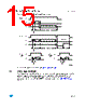
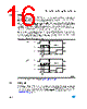
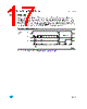
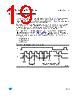
16 / 38 page  Instructions M93C86, M93C76, M93C66, M93C56, M93C46 16/38 5.4 Write For the Write Data to Memory (WRITE) instruction, 8 or 16 data bits follow the op-code and address bits. These form the byte or word that is to be written. As with the other bits, Serial Data Input (D) is sampled on the rising edge of Serial Clock (C). After the last data bit has been sampled, the Chip Select Input (S) must be taken low before the next rising edge of Serial Clock (C). If Chip Select Input (S) is brought low before or after this specific time frame, the self-timed programming cycle will not be started, and the addressed location will not be programmed. The completion of the cycle can be detected by monitoring the READY/BUSY line, as described later in this document. Once the Write cycle has been started, it is internally self-timed (the external clock signal on Serial Clock (C) may be stopped or left running after the start of a Write cycle). The cycle is automatically preceded by an Erase cycle, so it is unnecessary to execute an explicit erase instruction before a Write Data to Memory (WRITE) instruction. Figure 5. ERASE, ERAL sequences 1. For the meanings of An and Xn, please see Table 5., Table 6. and Table 7.. 5.5 Erase All The Erase All Memory (ERAL) instruction erases the whole memory (all memory bits are set to 1). The format of the instruction requires that a dummy address be provided. The Erase cycle is conducted in the same way as the Erase instruction (ERASE). The completion of the cycle can be detected by monitoring the READY/BUSY line, as described in the READY/BUSY status section. AI00879B S ERASE 1 1 D Q ADDR OP CODE 1 BUSY READY CHECK STATUS S ERASE ALL 1 0 D Q OP CODE 1 BUSY READY CHECK STATUS 0 0 An A0 Xn X0 ADDR |
|
Link URL |
| Cho đến nay ALLDATASHEET có giúp ích cho doanh nghiệp của bạn hay không? [ DONATE ] |
Alldatasheet là | Quảng cáo | Liên lạc với chúng tôi | Chính sách bảo mật | Liên kết đến bảng dữ liệu | Trao đổi link | Tìm kiếm theo nhà sản xuất All Rights Reserved©Alldatasheet.com |
| Russian : Alldatasheetru.com | Korean : Alldatasheet.co.kr | Spanish : Alldatasheet.es | French : Alldatasheet.fr | Italian : Alldatasheetit.com Portuguese : Alldatasheetpt.com | Polish : Alldatasheet.pl | Vietnamese : Alldatasheet.vn Indian : Alldatasheet.in | Mexican : Alldatasheet.com.mx | British : Alldatasheet.co.uk | New Zealand : Alldatasheet.co.nz |
|
Family Site : ic2ic.com |
icmetro.com |
 Vietnamese ▼
 English
 Chinese
 German
 Japanese
 Russian
 Korean
 Spanish
 French
 Italian
 Portuguese
 Polish
 Vietnamese
 Indian
 Mexican
 British
 New Zealand