|
công cụ tìm kiếm bảng dữ liệu linh kiện điện tử |
|
|
công cụ tìm kiếm bảng dữ liệu linh kiện điện tử |
|
UT7R995 bảng dữ liệu(PDF) 1 Page - Aeroflex Circuit Technology |
|
|
|||||||||||||||||||||||||||||
UT7R995 bảng dữ liệu(HTML) 1 Page - Aeroflex Circuit Technology |
|
|
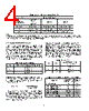
1 / 22 page  1 FEATURES: +3.3V Core Power Supply +2.5V or +3.3V Clock Output Power Supply - Independent Clock Output Bank Power Supplies Output frequency range: 6 MHz to 200 MHz Bank pair output-output skew < 100 ps Cycle-cycle jitter < 50 ps 50% ± 2% maximum output duty cycle at 100MHz Eight LVTTL outputs with selectable drive strength Selectable positive- or negative-edge synchronization Selectable phase-locked loop (PLL) frequency range and lock indicator Phase adjustments in 625 to 1300 ps steps up to ± 7.8 ns (1-6,8,10,12) x multiply and (1/2,1/4) x divide ratios Compatible with Spread-Spectrum reference clocks Power-down mode Selectable reference input divider Radiation performance - Total-dose tolerance: 100 krad (Si) - SEL Immune to a LET of 109 MeV-cm2/mg - SEU Immune to a LET of 109 MeV-cm2/mg Military temperature range: -55oC to +125oC Extended industrial temp: -40oC to +125oC Packaging options: - 48-Lead Ceramic Flatpack Standard Microcircuit Drawing: 5962-05214 - QML-Q and QML-V compliant part INTRODUCTION: The UT7R995/UT7R995C is a low-voltage, low-power, eight- output, 6-to-200 MHz clock driver. It features output phase programmability which is necessary to optimize the timing of high-performance microprocessor and communication sys- tems. The user programs both the frequency and the phase of the out- put banks through nF[1:0] and DS[1:0] pins. The adjustable phase feature allows the user to skew the outputs to lead or lag the reference clock. Connect any one of the outputs to the feedback input to achieve different reference frequency multi- plication and division ratios. The devices also feature split output bank power supplies that enable banks 1 & 2, bank 3, and bank 4 to operate at a different power supply levels. The ternary PE/HD pin controls the syn- chronization of output signals to either the rising or the falling edge of the reference clock and selects the drive strength of the output buffers. The UT7R995 and UT7R995C both interface to a digital clock while the UT7R995C will also interface to a quartz crystal. Figure 1. 48-Lead Ceramic Flatpack Pin Description 1 2 3 4 5 6 7 8 9 10 11 12 13 14 15 16 17 18 19 20 21 22 23 24 48 47 46 45 44 43 42 41 40 39 38 37 36 35 34 33 32 31 30 29 28 27 26 25 4F0 4F1 sOE PD/DIV PE/HD VDD VDDQ3 3Q1 3Q0 VSS VSS VDD FB VDD VSS VSS 2Q1 2Q0 VDDQ1 LOCK VSS DS0 DS1 1F0 3F1 3F0 FS VSS VSS VDDQ4 4Q1 4Q0 VSS VSS VDD XTAL1 NC/XTAL2 VDD VSS VSS 1Q1 1Q0 VDDQ1 VSS TEST 2F1 2F0 1F1 UT7R995 & UT7R995C Standard Products UT7R995 & UT7R995C RadClockTM RadHard 2.5V/3.3V 200MHz High-Speed Multi-phase PLL Clock Buffer Datasheet February, 2007 |
Số phần tương tự - UT7R995 |
|
Mô tả tương tự - UT7R995 |
|
|
|
Link URL |
| Cho đến nay ALLDATASHEET có giúp ích cho doanh nghiệp của bạn hay không? [ DONATE ] |
Alldatasheet là | Quảng cáo | Liên lạc với chúng tôi | Chính sách bảo mật | Liên kết đến bảng dữ liệu | Trao đổi link | Tìm kiếm theo nhà sản xuất All Rights Reserved©Alldatasheet.com |
| Russian : Alldatasheetru.com | Korean : Alldatasheet.co.kr | Spanish : Alldatasheet.es | French : Alldatasheet.fr | Italian : Alldatasheetit.com Portuguese : Alldatasheetpt.com | Polish : Alldatasheet.pl | Vietnamese : Alldatasheet.vn Indian : Alldatasheet.in | Mexican : Alldatasheet.com.mx | British : Alldatasheet.co.uk | New Zealand : Alldatasheet.co.nz |
|
Family Site : ic2ic.com |
icmetro.com |
 Vietnamese ▼
 English
 Chinese
 German
 Japanese
 Russian
 Korean
 Spanish
 French
 Italian
 Portuguese
 Polish
 Vietnamese
 Indian
 Mexican
 British
 New Zealand