|
công cụ tìm kiếm bảng dữ liệu linh kiện điện tử |
|
|
công cụ tìm kiếm bảng dữ liệu linh kiện điện tử |
|
PI2DPX2020 bảng dữ liệu(PDF) 21 Page - Diodes Incorporated |
|
|
|||||||||||||||||||||||||||||
PI2DPX2020 bảng dữ liệu(HTML) 21 Page - Diodes Incorporated |
|
|
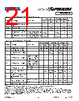
21 / 39 page  A Product Line of Diodes Incorporated PI2DPX2020 21 www.diodes.com July 2022 Diodes Incorporated PI2DPX2020 Document Number DS43506 Rev 5-2 Symbol Parameter Conditions This Silicon Fast-mode Plus Spec Units Min. Max. Min. Max. Cb Capacitive load for each bus line - 550 - 550 pF tVD;DAT Data valid time - 0.45 - 0.45 us tVD;ACK Data valid acknowledge time - 0.45 - 0.45 us VnL Noise margin at the LOW level For each connected device (including hysteresis) 0.1VDD 0.1VDD - V VnH Noise margin at the HIGH level For each connected device (including hysteresis) 0.2VDD 0.2VDD - V Characteristics of the SDA and SCL Bus Lines the Devices Cont. Characteristics of the SDA and SCL I/O Stages Symbol Parameter Conditions Standard-mode Fast-mode Fast-mode Plus Units Min. Max. Min. Max. Min. Max. VIL LOW-level input voltage(1) -0.5 0.3VDD -0.5 0.3VDD -0.5 0.3VDD V VIH HIGH-level input voltage(1) 0.7VDD (2) 0.7VDD (2) 0.7VDD(1) (2) V Vhys Hysteresis of Schmitt trigger inputs 0.05VDD 0.05VDD V VOL1 LOW-level output voltage 1 Open-drain or open- collector at 3mA sink current; VDD > 2V 0 0.4 0 0.4 0 0.4 V VOL2 LOW-level output voltage 2 Open-drain or open- collector at 2mA sink current(3); VDD ≤ 2V 0 0.2VDD 0 0.2VDD V IOL LOW-level output current VOL =0.4V 3 3 20 mA VOL =0.6V(4) 6 tof Output fall time from VIHmin to VILmax 250(5) 20×(VDD /5.5V)(6) 250 (5) 20×(VDD /5.5V)(6) 120 (7) ns tSP Pulse width of spikes that must be suppressed by the input filter 0 50(8) 0 50(8) ns Ii Input current each I/O pin 0.1VDD <VI < 0.9VD- Dmax -10 +10 -10(9) +10(9) -10(9) +10(9) µA Ci Capacitance for each I/O pin(10) 10 10 10 pF Note: 1. Some legacy Standard-mode devices had fixed input levels of VIL = 1.5V and VIH = 3.0V. Refer to component datasheet. 2. Maximum VIH = VDD(max) + 0.5V or 5.5V, which ever is lower. See component datasheet. 3. The same resistor value to drive 3mA at 3.0V VDD provides the same RC time constant when using <2V VDD with a smaller current draw. 4. In order to drive full bus load at 400kHz, 6mA IOL is required at 0.6V VOL. Parts not meeting this specification can still function, but not at 400kHz and 400pF. 5. The maximum tf for the SDA and SCL bus lines quoted in Table 10 (300ns) is longer than the specified maximum tof for the output stages (250ns). This allows series protection resistors (RS) to be connected between the SDA/SCL pins and the SDA/SCL bus lines as shown in Figure 45 without exceeding the maximum specified tf. 6. Necessary to be backwards compatible with Fast-mode. |
|
Link URL |
| Cho đến nay ALLDATASHEET có giúp ích cho doanh nghiệp của bạn hay không? [ DONATE ] |
Alldatasheet là | Quảng cáo | Liên lạc với chúng tôi | Chính sách bảo mật | Liên kết đến bảng dữ liệu | Trao đổi link | Tìm kiếm theo nhà sản xuất All Rights Reserved©Alldatasheet.com |
| Russian : Alldatasheetru.com | Korean : Alldatasheet.co.kr | Spanish : Alldatasheet.es | French : Alldatasheet.fr | Italian : Alldatasheetit.com Portuguese : Alldatasheetpt.com | Polish : Alldatasheet.pl | Vietnamese : Alldatasheet.vn Indian : Alldatasheet.in | Mexican : Alldatasheet.com.mx | British : Alldatasheet.co.uk | New Zealand : Alldatasheet.co.nz |
|
Family Site : ic2ic.com |
icmetro.com |
 Vietnamese ▼
 English
 Chinese
 German
 Japanese
 Russian
 Korean
 Spanish
 French
 Italian
 Portuguese
 Polish
 Vietnamese
 Indian
 Mexican
 British
 New Zealand