|
công cụ tìm kiếm bảng dữ liệu linh kiện điện tử |
|
|
công cụ tìm kiếm bảng dữ liệu linh kiện điện tử |
|
AS1130 bảng dữ liệu(PDF) 16 Page - ams AG |
|
|
|||||||||||||||||||||||||||||
AS1130 bảng dữ liệu(HTML) 16 Page - ams AG |
|
|
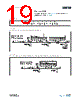
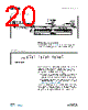
16 / 66 page  Page 16 ams Datasheet Document Feedback [v2-01] 2016-Oct-12 AS1130 − Detailed Description Cross-Plexing Theorem The cross-plexing theorem is using the fact that a LED has a forward and backward direction. A LED will only glow if there is a current flowing in forward direction. A parallel LED in backward direction will block the current flow. This effect is used in a cross-plexed matrix of LEDs. Each CSx pin (CS0 to CS11) can be switched to VDD via the internal current source (“high”), to GND (“low”) or not connected (“highZ”). The mode of operation which is controlled by an internal state machine looks like following. CS0 is switched to GND and all other CSx pins (CS1 to CS11) are controlled according to the settings in the On/Off Frame and Blink & PWM registers (see Figure 31). Than CS1 is switched to GND and all other CSx pins (CS0 and CS2 to CS11) are controlled according to the settings in the On/Off Frame and Blink & PWM registers. In this manner all LEDs in the matrix are scanned and turned on/off depending on the register settings. I²C Interface The AS1130 supports the I²C serial bus and data transmission protocol in fast mode at 1MHz. The AS1130 operates as a slave on the I²C bus. The bus must be controlled by a master device that generates the serial clock (SCLK), controls the bus access, and generates the START and STOP conditions. Connections to the bus are made via the open-drain I/O pins SCLK and SDA. Figure 23: I²C Interface Initialization Detailed Description 19 81 9 8 1 0 AD2 10 AD1 AD0 R/W D15 D14 D13 D12 D11 D10 D9 D8 AD2, AD1 and AD0 are defined by the pin ADDR, see I²C Device Address Byte. SCLK SDA |
|
Link URL |
| Cho đến nay ALLDATASHEET có giúp ích cho doanh nghiệp của bạn hay không? [ DONATE ] |
Alldatasheet là | Quảng cáo | Liên lạc với chúng tôi | Chính sách bảo mật | Liên kết đến bảng dữ liệu | Trao đổi link | Tìm kiếm theo nhà sản xuất All Rights Reserved©Alldatasheet.com |
| Russian : Alldatasheetru.com | Korean : Alldatasheet.co.kr | Spanish : Alldatasheet.es | French : Alldatasheet.fr | Italian : Alldatasheetit.com Portuguese : Alldatasheetpt.com | Polish : Alldatasheet.pl | Vietnamese : Alldatasheet.vn Indian : Alldatasheet.in | Mexican : Alldatasheet.com.mx | British : Alldatasheet.co.uk | New Zealand : Alldatasheet.co.nz |
|
Family Site : ic2ic.com |
icmetro.com |
 Vietnamese ▼
 English
 Chinese
 German
 Japanese
 Russian
 Korean
 Spanish
 French
 Italian
 Portuguese
 Polish
 Vietnamese
 Indian
 Mexican
 British
 New Zealand