|
công cụ tìm kiếm bảng dữ liệu linh kiện điện tử |
|
|
công cụ tìm kiếm bảng dữ liệu linh kiện điện tử |
|
ADP2291ACPZ-R7 bảng dữ liệu(PDF) 12 Page - Analog Devices |
|
|
|||||||||||||||||||||||||||||
ADP2291ACPZ-R7 bảng dữ liệu(HTML) 12 Page - Analog Devices |
|
|
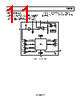
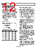
12 / 20 page  ADP2291 Rev. 0 | Page 12 of 20 APPLICATION INFORMATION SETTING THE MAXIMUM CHARGE CURRENT The maximum charge current is set by choosing the proper current sense resistor, RS, and the voltage on the ADJ input. The charger nominally regulates its output current at the point where the voltage across the current sense resistor VIN–VCS (defined as VRS) is 150 mV. This setpoint voltage can be adjusted by pulling down on the ADJ input, which is internally attached through a 100 kΩ pull-up resistor to 3 V. Each volt of pull-down from 3 V will reduce VRS by 67 mV during fast charge. A minimum of 50 mV is reached when a 100 kΩ resistor is attached between ADJ and ground. During slow charge the voltage across the current sense resistor is 15 mV with no connection to ADJ and drops to 10 mV with a 100 kΩ resistor attached to ground. Therefore the maximum charge rate IMAX can be calculated as ) mΩ ( ) mV ( S RS MAX R V I = (1) where 50 mV ≤ VRS ≤ 150 mV After determining suitable values for VRS and RS, the value of VADJ and RADJ can be calculated as V V V RS ADJ mV 7 . 66 mV 50 ) mV ( + = (2) RADJ = 100 kΩ × ⎟ ⎠ ⎞ ⎜ ⎝ ⎛ − ADJ ADJ V V V 3 (3) Examples of resistor combinations are shown in Table 4. Table 4. Examples of RS and RADJ Selection IMAX RS VRS VADJ RADJ 1.5 A 100 mΩ 150 mV 3 V Open 1 A 100 mΩ 100 mV 2.25 V 300 K 750 mA 100 mΩ 75 mV 1.87 V 167 K 500 mA 100 mΩ 50 mV 1.5 V 100 K 750 mA 200 mΩ 150 mV 3 V Open 500 mA 200 mΩ 100 mV 2.25 V 300 K 375 mA 200 mΩ 75 mV 1.87 V 167 K 250 mA 200 mΩ 50 mV 1.5 V 100 K 500 mA 300 mΩ 150 mV 3 V Open 333 mA 300 mΩ 100 mV 2.25 V 300 K 250 mA 300 mΩ 75 mV 1.87 V 167 K 167 mA 300 mΩ 50 mV 1.5 V 100 K SETTING THE MAXIMUM CHARGE TIME The maximum charge time is intended as a safety mechanism to prevent the charger from trickle charging the cell indefinitely. It does not terminate charging under normal charging conditions, but only when there is a failure to reach end-of-charge. A typical cell charges at a 1 C rate in about 1.5 hours, depending on the cell type, temperature, and manufacturer. Generally, a three hour time limit is sufficient to prevent a normal charge cycle from being interrupted by the charge timer. It is recommended that the cell manufacturer be consulted for timing details. The maximum charge time is set by selecting the value of the CTIMER capacitor. Calculate the timer capacitance using CTIMER = tCHG(minutes) × minutes 1800 1 F µ (4) The precharge and end-of-charge periods are 1/6 the duration of the fast charge time limit. The charge timers are completely disabled by connecting the TIMER pin to ground. If the timers are disabled, the FAULT and TIMEOUT states are never reached, so the timers should only be disabled if charging is monitored and controlled externally. EXTERNAL CAPACITORS Use an input supply capacitor (CIN) with a value in the 1 µF to 10 µF range and place it close to the ADP2291. This should provide adequate input bypassing, but the selected capacitor should be checked in the actual application circuit. Check that the input voltage does not droop or overshoot excessively during the start-up transient. Use a battery output capacitor (COUT) with a value of at least 10 µF. This capacitance provides compensation when no battery load is present. In addition, the battery and interconnections appear inductive at high frequencies and must be accounted for when the charger is operated with a battery load. Therefore, a small amount of output capacitance is necessary to compensate for the inductive nature of the battery and connections. Use a minimum output capacitance value of 1 µF for applications where the battery cannot be removed. REVERSE INPUT PROTECTION The diode, D1, shown in Figure 22 through Figure 25 is optional. It is only required if the input adapter voltage can be applied with a reverse polarity. If the adapter voltage is high enough, a Schottky diode is recom- mended to minimize the voltage difference from the adapter to the charger input and the power dissipation. Choose a diode with a continuous current rating high enough to handle battery charging current at the maximum ambient temperature. Use a diode whose voltage rating is greater than the maximum adapter voltage. |
|
|
Link URL |
| Cho đến nay ALLDATASHEET có giúp ích cho doanh nghiệp của bạn hay không? [ DONATE ] |
Alldatasheet là | Quảng cáo | Liên lạc với chúng tôi | Chính sách bảo mật | Liên kết đến bảng dữ liệu | Trao đổi link | Tìm kiếm theo nhà sản xuất All Rights Reserved©Alldatasheet.com |
| Russian : Alldatasheetru.com | Korean : Alldatasheet.co.kr | Spanish : Alldatasheet.es | French : Alldatasheet.fr | Italian : Alldatasheetit.com Portuguese : Alldatasheetpt.com | Polish : Alldatasheet.pl | Vietnamese : Alldatasheet.vn Indian : Alldatasheet.in | Mexican : Alldatasheet.com.mx | British : Alldatasheet.co.uk | New Zealand : Alldatasheet.co.nz |
|
Family Site : ic2ic.com |
icmetro.com |
 Vietnamese ▼
 English
 Chinese
 German
 Japanese
 Russian
 Korean
 Spanish
 French
 Italian
 Portuguese
 Polish
 Vietnamese
 Indian
 Mexican
 British
 New Zealand