|
công cụ tìm kiếm bảng dữ liệu linh kiện điện tử |
|
|
công cụ tìm kiếm bảng dữ liệu linh kiện điện tử |
|
ICS342 bảng dữ liệu(PDF) 3 Page - Integrated Device Technology |
|
|
|||||||||||||||||||||||||||||
ICS342 bảng dữ liệu(HTML) 3 Page - Integrated Device Technology |
|
|
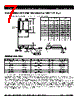
3 / 9 page  ICS342 FIELD PROGRAMMABLE DUAL OUTPUT SS VERSACLOCK SYNTHESIZER EPROM CLOCK SYNTHESIZER IDT® / ICS™ FIELD PROGRAMMABLE DUAL OUTPUT SS VERSACLOCK SYNTHESIZER 3 ICS342 REV N 090613 3) To minimize EMI, the 33 series termination resistor (if needed) should be placed close to the clock output. 4) An optimum layout is one with all components on the same side of the board, minimizing vias through other signal layers. Other signal traces should be routed away from the ICS342. This includes signal traces just underneath the device, or on layers adjacent to the ground plane layer used by the device. ICS342 Configuration Capabilities The architecture of the ICS342 allows the user to easily configure the device to a wide range of output frequencies, for a given input reference frequency. The frequency multiplier PLL provides a high degree of precision. The M/N values (the multiplier/divide values available to generate the target VCO frequency) can be set within the range of M = 1 to 2048 and N = 1 to 1024. The ICS342 also provides separate output divide values, from 2 through 20, to allow the two output clock banks to support widely differing frequency values from the same PLL. Each output frequency can be represented as: IDT VersaClock Software IDT applies years of PLL optimization experience into a user friendly software that accepts the user’s target reference clock and output frequencies and generates the lowest jitter, lowest power configuration, with only a press of a button. The user does not need to have prior PLL experience or determine the optimal VCO frequency to support multiple output frequencies. VersaClock software quickly evaluates accessible VCO frequencies with available output divide values and provides an easy to understand, bar code rating for the target output frequencies. The user may evaluate output accuracy, performance trade-off scenarios in seconds. Spread Spectrum Modulation The ICS342 utilizes frequency modulation (FM) to distribute energy over a range of frequencies. By modulating the output clock frequencies, the device effectively lowers energy across a broader range of frequencies; thus, lowering a system’s electromagnetic interference (EMI). The modulation rate is the time from transitioning from a minimum frequency to a maximum frequency and then back to the minimum. Spread Spectrum Modulation can be applied as either “center spread” or “down spread”. During center spread modulation, the deviation from the target frequency is equal in the positive and negative directions. The effective average frequency is equal to the target frequency. In applications where the clock is driving a component with a maximum frequency rating, down spread should be applied. In this case, the maximum frequency, including modulation, is the target frequency. The effective average frequency is less than the target frequency. The ICS342 operates in both center spread and down spread modes. For center spread, the frequency can be modulated between +/- 0.125% to +/-2.0%. For down spread, the frequency can be modulated between -0.25% to -4.0%. Both output frequency banks will utilize identical spread spectrum percentage deviations and modulation rates, if a common VCO frequency can be identified. Spread Spectrum Modulation Rate The spread spectrum modulation frequency applied to the output clock frequency may occur at a variety of rates. For applications requiring the driving of “down-circuit” PLLs, Zero Delay Buffers, or those adhering to PCI standards, the spread spectrum modulation rate should be set to 30-33 kHz. For other applications, a 120 kHz modulation option is available. Using VersaClock Products with an Input Clock Source In order to ensure proper startup with an input clock rather than a crystal, the supply voltage must be within the operating range (3.3V ±10%) and the input signal must be stable and free from glitching. The input clock must provide pulses of at least 20ns, and no more than 500ns, for at least 160 clock cycles without any interruptions to the clock or power during this period. It may take up to 4ms for output frequencies to reach their target frequency values. An alternative method is to have the PDTS pin asserted low while power supplies and clock sources stabilize.Once the power supply and input clock source are constant and within the acceptable frequency range, bring PDTS high. This approach is preferred if the clock source is derived from another PLL, or the source oscillator produces unpredictable output pulses prior to stabilization. No considerations need to be taken when using a crystal input source with VersaClock products. OutputFreq REFFreq OutputDivide -------------------------------------- M N ----- = |
|
|
Link URL |
| Cho đến nay ALLDATASHEET có giúp ích cho doanh nghiệp của bạn hay không? [ DONATE ] |
Alldatasheet là | Quảng cáo | Liên lạc với chúng tôi | Chính sách bảo mật | Liên kết đến bảng dữ liệu | Trao đổi link | Tìm kiếm theo nhà sản xuất All Rights Reserved©Alldatasheet.com |
| Russian : Alldatasheetru.com | Korean : Alldatasheet.co.kr | Spanish : Alldatasheet.es | French : Alldatasheet.fr | Italian : Alldatasheetit.com Portuguese : Alldatasheetpt.com | Polish : Alldatasheet.pl | Vietnamese : Alldatasheet.vn Indian : Alldatasheet.in | Mexican : Alldatasheet.com.mx | British : Alldatasheet.co.uk | New Zealand : Alldatasheet.co.nz |
|
Family Site : ic2ic.com |
icmetro.com |
 Vietnamese ▼
 English
 Chinese
 German
 Japanese
 Russian
 Korean
 Spanish
 French
 Italian
 Portuguese
 Polish
 Vietnamese
 Indian
 Mexican
 British
 New Zealand